New Semester
Started
Get
50% OFF
Study Help!
--h --m --s
Claim Now
Question Answers
Textbooks
Find textbooks, questions and answers
Oops, something went wrong!
Change your search query and then try again
S
Books
FREE
Study Help
Expert Questions
Accounting
General Management
Mathematics
Finance
Organizational Behaviour
Law
Physics
Operating System
Management Leadership
Sociology
Programming
Marketing
Database
Computer Network
Economics
Textbooks Solutions
Accounting
Managerial Accounting
Management Leadership
Cost Accounting
Statistics
Business Law
Corporate Finance
Finance
Economics
Auditing
Tutors
Online Tutors
Find a Tutor
Hire a Tutor
Become a Tutor
AI Tutor
AI Study Planner
NEW
Sell Books
Search
Search
Sign In
Register
study help
computer science
digital systems principles and application
Digital Systems Principles And Application 12th Edition Ronald Tocci, Neal Widmer, Gregory Moss - Solutions
True or false: Clock waveforms with too great of a rise time or fall time may not trigger the flip-flop reliably.
In VHDL, what serves as “wires” that connect components?
True or false: Metastable states are the greatest benefit of using clock flip-flops.
If this counter starts at 00000000, what will be its state after 520 pulses?
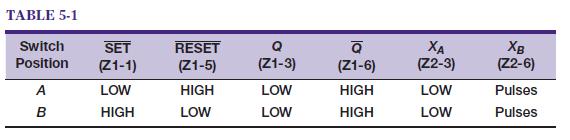
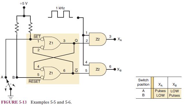
A technician tests the circuit of Figure 5-13 and records the observations shown in Table 5-1. He notices that when the switch is in position B, the circuit functions correctly, but in position A the latch does not set to the Q = 1 state. What are the possible faults that could produce this
In VHDL, what keyword identifies the section of code where connections are specified for instances of components?
Which library defines the logic primitives and common components?
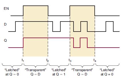
Determine the Q waveform for a D latch with the EN and D inputs of Figure 5-31. Assume that Q = 0 initially.Figure 5-31 ΕΝ D Q "Latched" at Q = 0 1 "Transparent" Q=D "Latched" at Q=1 13 "Transparent" Q =D 14 "Latched" at Q = 0
When a microcontroller wants to access data in its external memory, it activates an active-LOW output pin called R̅D̅ (read). The data book says that the R̅D̅ pulse typically has a pulse width tw of 50 ns, a rise time tr of 15 ns, and a fall time tf of 10 ns. Draw a scaled drawing of the R̅D̅
What causes a flip-flop to exhibit a metastable state?
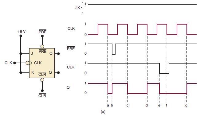
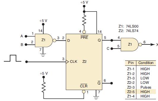
Figure 5-33(a) shows the symbol for a J-K FF that responds to a NGT on its clock input and has active-LOW asynchronous inputs. The external active- LOW asynchronous inputs are labeled PRE and CLR. The bubble on an input means that the input responds to a logic LOW signal. The J and K inputs are
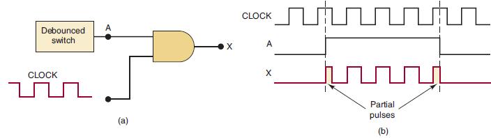
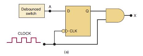
Figure 5-38(a) shows a situation where input signal A is generated from a debounced switch that is actuated by an operator (a debounced switch was first introduced in Example 5-2). A goes HIGH when the operator actuates the switch and goes LOW when the operator releases the switch. This A input is
Consider a counter circuit that contains six FFs wired in the arrangement of Figure 5-48 (i.e., Q5, Q4, Q3, Q2, Q1, Q0).(a) Determine the counter’s MOD number.(b) Determine the frequency at the output of the last FF (Q5) when the input clock frequency is 1 MHz.(c) What is the range of counting
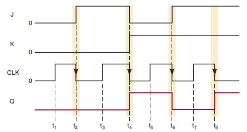
Determine the Q output for a negative-edge-triggered J-K flip-flop for the input waveforms shown in Figure 5-37. Assume that tH = 0 and that Q = 0 initially.Figure 5-37 K CLK Q 0 0 I
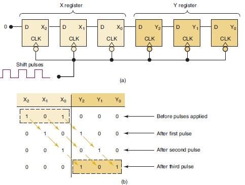
Assume the same initial contents of the X and Y registers in Figure 5-47. What will be the contents of each FF after the occurrence of the sixth shift pulse?Figure 5-47 D Shift pulses X₂ 0 CLK 0 0 X register D 9 O 000 X₁ CLK 0 n D 0 0 1 Xo CLK Yo 0 0 (a) 0 (b) D CLK Y register D Y₁ CLK Before
Review the material in Section 2-5 regarding quadrature shaft encoder signals. Recall that a quadrature shaft encoder produces two output signals that are shifted 90 degrees. If the shaft rotates one direction, output A will lead output B. If it rotates in the other direction, output A will lag
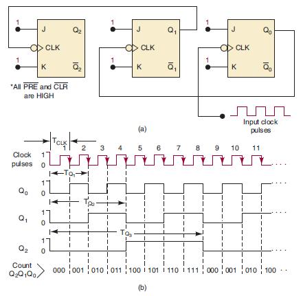
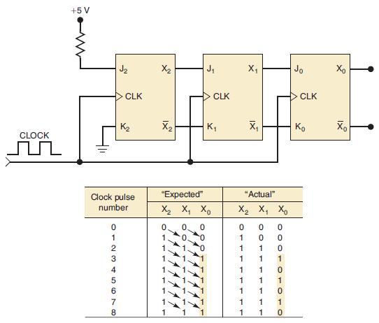
Assume that the MOD-8 counter in Figure 5-48 is in the 101 state. What will be the state (count) after 13 pulses have been applied?Figure 5-48 1 J O CLK K *All PRE and CLR are HIGH Q₁ Clock pulses 0 Qo 0 0 Q₂ 0 Count Q₂Q100/ TCLK -To₁- 1 1 2 Toe 3 4 TO₂ J CLK K (a) Q₁ Q₁ 1 I J O
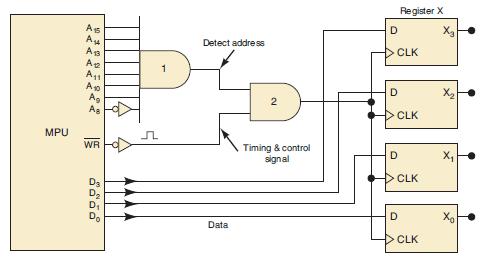
(a) What address code must the MPU in Figure 5-58 generate in order for the data to be transferred into register X?(b) Assume that X3 – X0 = 0110, A15 – A8 = 11111111, and D3 – D0 = 1011. What will be in X after a WR pulse occurs?Figure 5-58 MPU As >>>> 109 13
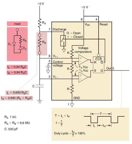
Using the diodes along with RB as shown in Figure 5-64, calculate the values of RA and RB necessary to get a 1 kHz, 25 percent duty cycle waveform out of a 555. Assume C is a 0.1 μF capacitor.Figure 5-64 Inset Rg D₁ 01730₂ 0.94 R₂C = 0.94 RAC ¹L = 0.693 RBC TH=0.693 (R₂ + Rg)C RA 1 KQ RA
Figure 5-65 shows a three-bit shift register made up of TTL flip-flops. Initially, all of the FFs are in the LOW state before clock pulses are applied. As clock pulses are applied, each PGT will cause the information to shift from each FF to the one on its right. The diagram shows the
Calculate the frequency and the duty cycle of the 555 astable multivibrator output for C = 0.001 μF, RA = 2.2 kΩ, and RB = 100 kΩ.
Consider the circuit in Figure 5-66 and examine the logic probe indications shown in the accompanying table. There is a LOW at the D input of the FF when pulses are applied to its CLK input, but the Q output fails to go to the LOW state. The technician testing this circuit considers each of the
Compare the operation of a level-enabled D latch and an edge-triggered D flip-flop using the Quartus functional simulator.
Construct a block description file (bdf) of a register that consists of four D flip-flops using the DFF primitive. From this BDF file, create a block symbol and include it in a new design. The new design will have inputs named D[3..0], TRANSFER (clock input), and Q[3..0]. Determine its operation
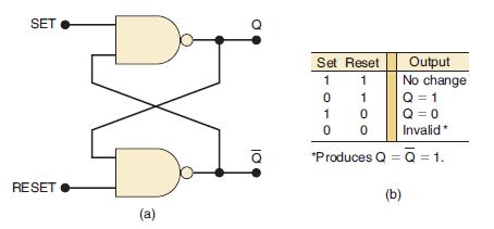
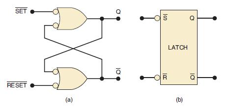
Describe an active-LOW input S-R latch with inputs named SBAR, RBAR, and one output named Q. It should follow the function table of a NAND latch (see Figure 5-6) and the invalid input combination should produce Q = 1.(a) Use AHDL.(b) Use VHDL.Figure 5-6 SET RESET (a) Q 10 Set Reset Output No
What are the names of the three Quartus libraries that contain useful functions for logic systems.
How does the operation of an asynchronous input differ from that of a synchronous input?
Describe how a D latch operates differently from an edge-triggered D flip-flop.
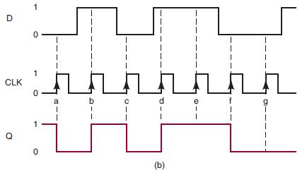
What will happen to the Q waveform in Figure 5-27(b) if the D input is held permanently LOW?Figure 5-27(b) D CLK 1 0 1 0 1 0 I a b 1 1 с (b) e 1 A AL 1
What is clock skew? How can it cause a problem?
Determine the approximate frequency of a Schmitt-trigger oscillator that uses a 74HC14 with R = 10 kΩ and C = 0.005 μF.
True or false: A J-K flip-flop can be used as an S-R flip-flop, but an S-R flip-flop cannot be used as a J-K flip-flop.
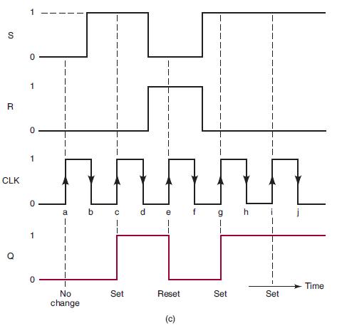
Suppose that the waveforms of Figure 5-20(c) are applied to the inputs of the FF of Figure 5-21. What will happen to Q at point b? At point f? At point h?Figure 5-20 (c)Figure 5-21 S R CLK Q 1 0 0 1 0 No change b Set Reset (c) f 9 Set h I Set Time
In the absence of a trigger pulse, what will be the state of a OS output?
What could occur when a slow-changing signal is applied to a standard logic IC?
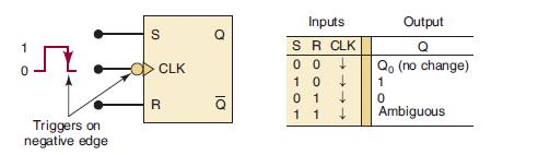
What two types of inputs does a clocked FF have?
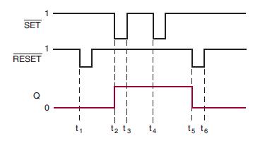
The waveforms of Figure 5-8 are applied to the inputs of the latch of Figure 5-7. Assume that initially Q = 0, and determine the Q waveform.Figure 5-7Figure 5-8 SET RESET (a) 10 -OS OR LATCH (b) Q 10
Define the following: rise time, fall time, rising edge, falling edge, leading edge, trailing edge, positive pulse, negative pulse, pulse width.
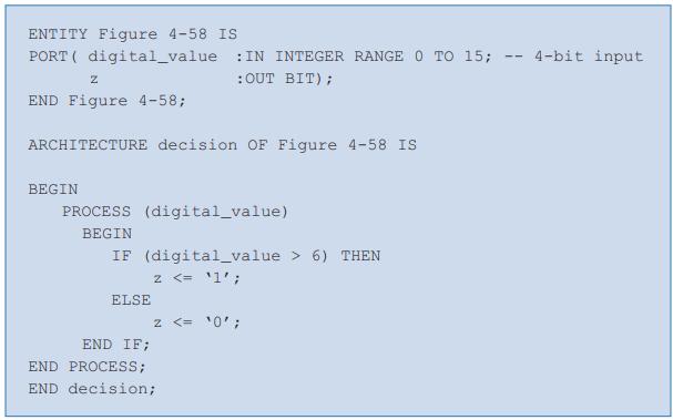
Modify the VHDL design in Figure 4-58 so that z = 1 only when the digital value is less than 10102.Figure 4-58
What is a logic primitive?
True or false: The fastest method for transferring data from one register to another is parallel transfer.
What is the normal resting state of the S̅E̅T̅ and R̅E̅S̅E̅T̅ inputs? What is the active state of each input?
Can the same component be used more than once in the same circuit?
What is the normal resting state of the NOR latch inputs? What is the active state?
A 20-kHz clock signal is applied to a J-K flip-flop with J = K = 1. What is the frequency of the FF output waveform?
(a) Determine the output waveform for the circuit of Figure 4-73.(b) Repeat with the B input held LOW.(c) Repeat with B held HIGH.Figure 4-73 0 1 1 Time 1 1 I m A B X
Determine the input conditions needed to produce x = 1 in Figure 4-74.Figure 4-74 A B TF с. X
Design a circuit that produces a HIGH output only when all three inputs are the same level.(a) Use a truth table and K map to produce the SOP solution.(b) Use two-input XOR and other gates to find a solution. (Recall the transitive property from algebra… if a = b and b = c then a = c.)
Modify the circuit of Figure 4-23 to compare two four-bit numbers and produce a HIGH output when the two numbers match exactly.Figure 4-23 Binary number Binary number ХО Y₁ Yo Z
A 7486 chip contains four XOR gates. Show how to make an XNOR gate using only a 7486 chip.
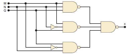
Figure 4-75 represents a relative-magnitude detector that takes two three-bit binary numbers, x2x1x0 and y2y1y0, and determines whether they are equal and, if not, which one is larger. There are three outputs, defined as follows:1. M = 1 only if the two input numbers are equal.2. N = 1 only if
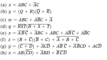
Simplify the following expressions using Boolean algebra. (a) x = ABC + AC (b) y (Q + R) (Q + R) (c) w = ABC + ABC + A (d) q = RST(R + S + T) = (e) x = ABC + ABC + ABC + ABC + ABC (f) 2 (B+C)(B+C) + A + B + C (g) y = (C+D) + ACD + ABC + ABCD + ACD (h) x = AB(CD) + ABD + BCD
Simplify the circuit of Figure 4-68 using Boolean algebra.Figure 4-68 MZO
Change each gate in Problem 4-2 to a NOR gate, and simplify the circuit using Boolean algebra.Data from Problem 4-2Simplify the circuit of Figure 4-68 using Boolean algebra.Figure 4-68 MZO
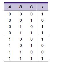
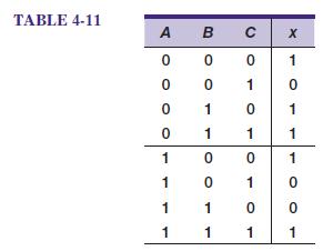
Design the logic circuit corresponding to the truth table shown in Table 4-11.Data from Table 4-11 А 0 0 0 0 1 1 1 1 В 0 0 1 0 0 1 1 с 0 1 0 1 0 1 0 1 X 1 0 1 1 1 0 0 1
Design a logic circuit whose output is HIGH only when a majority of inputs A, B, and C are LOW.
A manufacturing plant needs to have a horn sound to signal quitting time. The horn should be activated when either of the following conditions is met:1. It’s after 5 o’clock and all machines are shut down.2. It’s Friday, the production run for the day is complete, and all machines are shut
A four-bit binary number is represented as A3A2A1A0, where A3, A2, A1, and A0 represent the individual bits and A0 is equal to the LSB. Design a logic circuit that will produce a HIGH output whenever the binary number is greater than 0010 and less than 1000.
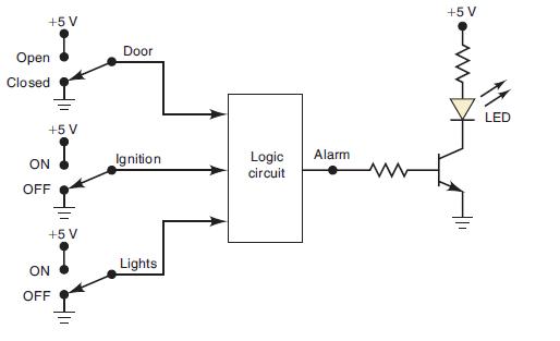
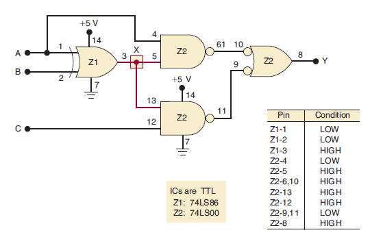
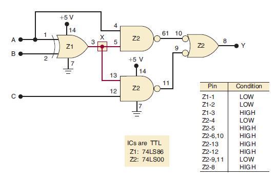
Figure 4-69 shows a diagram for an automobile alarm circuit used to detect certain undesirable conditions. The three switches are used to indicate the status of the door by the driver’s seat, the ignition, and the headlights, respectively. Design the logic circuit with these three switches as
Implement the circuit of Problem 4-4 using all NAND gates.Data from Problem 4-4Design the logic circuit corresponding to the truth table shown in Table 4-11.Data from Table 4-11 А 0 0 0 0 1 1 1 1 В 0 0 1 0 0 1 1 с 0 1 0 1 0 1 0 1 X 1 0 1 1 1 0 0 1
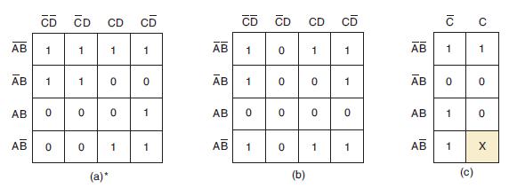
Determine the minimum expression for each K map in Figure 4-70. Pay particular attention to step 5 for the map in (a).Figure 4-70 AB AB CD CD АВ 1 AB 1 0 0 S 1 1 0 0 (a)* CD 1 0 0 1 CD 1 0 1 1 AB 1 Ав AB 18 AB 1 0 1 CD CD 0 0 0 1 0 0 0 (b) 1 CD 1 1 0 1 AB 9 AB 100 AB C C 1 0 1 1 (c) 1 0 0 X
Implement the circuit of Problem 4-5 using all NAND gates.Data from Problem 4-5Design a logic circuit whose output is HIGH only when a majority of inputs A, B, and C are LOW.
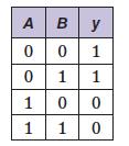
For the truth table below, create a 2 × 2 K map, group terms, and simplify. Then look at the truth table again to see if the expression is true for every entry in the table. ABY А 0 1 1 1 0 1 0 0 1 1 0 0
Starting with the truth table in Table 4-11, use a K map to find the simplest SOP equation. TABLE 4-11 A 0 0 0 0 1 1 1 1 в 0 0 1 1 0 0 1 1 с 0 1 0 1 0 1 0 1 X 1 0 1 1 1 0 0 1
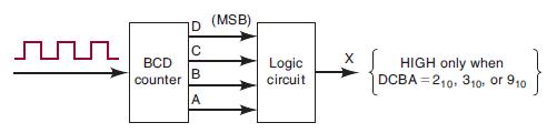
Figure 4-71 shows a BCD counter that produces a four-bit output representing the BCD code for the number of pulses that have been applied to the counter input. For example, after four pulses have occurred, the counter outputs are DCBA = 01002 = 410. The counter resets to 0000 on the tenth pulse and
Obtain the output expression for Problem 4-7 using a K map.Data from Problem 4-7A four-bit binary number is represented as A3A2A1A0, where A3, A2, A1, and A0 represent the individual bits and A0 is equal to the LSB. Design a logic circuit that will produce a HIGH output whenever the binary number
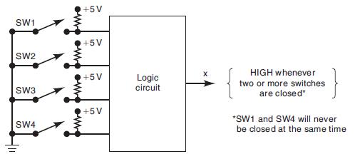
Figure 4-72 shows four switches that are part of the control circuitry in a copy machine. The switches are at various points along the path of the copy paper as the paper passes through the machine. Each switch is normally open, and as the paper passes over a switch, the switch closes. It is
Example 4-3 demonstrated algebraic simplification. Step 3 resulted in the SOP equation Use a K map to prove that this equation can be simplified further than the answer shown in the example.Data from Example 4-3 z = ABC + ACD + ABCD + ABC.
Use Boolean algebra to arrive at the same result obtained by the K map method of Problem 4-18.Problem 4-18Example 4-3 demonstrated algebraic simplification. Step 3 resulted in the SOP equation Use a K map to prove that this equation can be simplified further than the answer shown in the
Repeat Problem 3-17 for a NAND gate.Data from Problem 3-17Apply the input waveforms of Figure 3-54 to a NOR gate, and draw the output waveform.Repeat with C held permanently LOW.Repeat with C held HIGH.Figure 3-54 A B C . | | | | | -
Prove DeMorgan’s theorems by trying all possible cases.
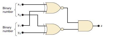
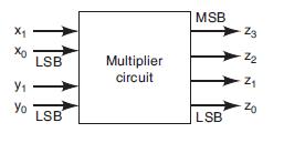
Figure 4-76 represents a multiplier circuit that takes two-bit binary numbers, x1x0 and y1y0, and produces an output binary number z3z2z1z0 that is equal to the arithmetic product of the two input numbers. Design the logic circuit for the multiplier.Figure 4-76
A BCD code is being transmitted to a remote receiver. The bits are A3, A2, A1, and A0, with A3 as the MSB. The receiver circuitry includes a BCD error detector circuit that examines the received code to see if it is a legal BCD code (i.e., ≤ 1001). Design this circuit to produce a HIGH for any
Design a logic circuit whose output is HIGH whenever A and B are both HIGH as long as C and D are either both LOW or both HIGH. Try to do this without using a truth table. Then check your result by constructing a truth table from your circuit to see if it agrees with the problem statement.
Four large tanks at a chemical plant contain different liquids being heated. Liquid-level sensors are being used to detect whenever the level in tank A or tank B rises above a predetermined level. Temperature sensors in tanks C and D detect when the temperature in either of these tanks drops below
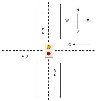
Figure 4-77 shows the intersection of a main highway with a secondary access road. Vehicle-detection sensors are placed along lanes C and D (main road) and lanes A and B (access road). These sensor outputs are LOW (0) when no vehicle is present and HIGH (1) when a vehicle is present. The
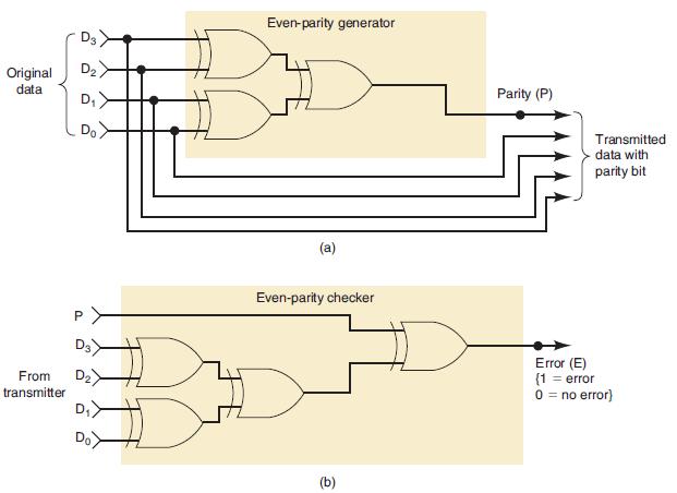
Redesign the parity generator and checker of Figure 4-25 to (a) Operate using odd parity. (b) Operate on eight data bits.Figure 4-25 D3 Original D₂ data D₁ Do PY D3 From D₂ transmitter D₁ Do Even-parity generator (a) Even-parity checker D (b) Parity (P) Transmitted data with parity
(a) Under what conditions will an OR gate allow a logic signal to pass through to its output unchanged?(b) Repeat (a) for an AND gate.(c) Repeat for a NAND gate.(d) Repeat for a NOR gate.
(a) Can an INVERTER be used as an enable/disable circuit? Explain.(b) Can an XOR gate be used as an enable/disable circuit? Explain.
Design a logic circuit that will allow input signal A to pass through to the output only when control input B is LOW while control input C is HIGH; otherwise, the output is LOW.
Design a logic circuit that controls the passage of signal A according to the following requirements:1. Output X will equal A when control inputs B and C are the same.2. X will remain HIGH when B and C are different.
Design a circuit that will disable the passage of an input signal only when control inputs B, C, and D are all HIGH; the output is to be HIGH in the disabled condition.
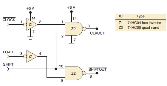
Assume that the ICs in Figure 4-32 are CMOS. Describe how the circuit operation would be affected by an open circuit in the conductor connecting Z2-2 and Z2-10.Figure 4-32 ܝܐܝ CLOCK 1 LOAD 3 SHIFT +5V 14 Z1 7 Z1 2 4 2 10 9 +5V 14 72 72 3 CLKOUT SHIFTOUT 8 IC 71 72 Type 74HC04 hex inverter 74HC00
In Example 4-24, we listed three possible faults for the situation of Figure 4-36. What procedure would you follow to determine which of the faults is the actual one?Example 4-24Refer to the circuit of Figure 4-36. A technician uses a logic probe to determine the conditions at the various IC pins.
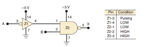
Refer to the circuit of Figure 4-38. Assume that the devices are CMOS. Also assume that the logic probe indication at Z2-3 is “indeterminate” rather than “pulsing.” List the possible faults, and write a procedure to follow to determine the actual fault.Figure 4-38 A B 3 Z1 4 1 2 Note: Vcc
Refer to the logic circuit of Figure 4-41. Recall that output Y is supposed to be HIGH for either of the following conditions:1. A = 1, B = 0, regardless of C 2. A = 0, B = 1, C = 1 When testing the circuit, the technician observes that Y goes HIGH only for the first condition but stays LOW for
Develop a procedure for isolating the fault that is causing the malfunction described in Problem 4-44.Data from Problem 4-44Refer to the logic circuit of Figure 4-41. Recall that output Y is supposed to be HIGH for either of the following conditions:1. A = 1, B = 0, regardless of C 2. A = 0, B =
Assume that the gates in Figure 4-41 are all CMOS. When the technician tests the circuit, he finds that it operates correctly except for the following conditions:1. A = 1, B = 0, C = 0 2. A = 0, B = 1, C = 1 For these conditions, the logic probe indicates indeterminate levels at Z2-6, Z2-11, and
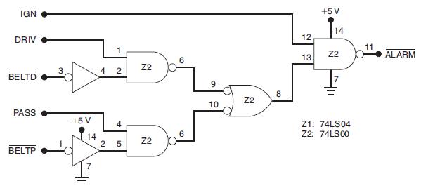
Figure 4-80 is a combinational logic circuit that operates an alarm in a car whenever the driver and/or passenger seats are occupied and the seatbelts are not fastened when the car is started. The active-HIGH signals DRIV and PASS indicate the presence of the driver and passenger, respectively, and
Suppose that the system of Figure 4-80 is functioning so that the alarm is activated as soon as the driver and/or passenger are seated and the car is started, regardless of the status of the seatbelts. What are the possible faults? What procedure would you follow to find the actual fault?Data
Suppose that the alarm system of Figure 4-80 is operating so that the alarm goes on continuously as soon as the car is started, regardless of the state of the other inputs. List the possible faults and write a procedure to isolate the fault.Data from Figure 4-80 IGN DRIV BELTD PASS BELTP 3 +5
True or false:(a) Top-down design begins with an overall description of the entire system and its specifications.(b) A JEDEC file can be used as the input file for a programmer.(c) If an input file compiles with no errors, it means the PLD circuit will work correctly.(d) A compiler can interpret
What are the % characters used for in the AHDL design file?
How are comments indicated in a VHDL design file?
What is a ZIF socket?
Name three entry modes used to input a circuit description into PLD development software
What do JEDEC and HDL stand for?
Declare the following data objects in AHDL or VHDL.(a) An array of eight output bits named gadgets.(b) A single-output bit named buzzer.(c) A 16-bit numeric input port named altitude.(d) A single, intermediate bit within a hardware description file named wire2.
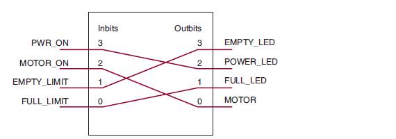
The following similar I/O definition is given for AHDL and VHDL.Write four concurrent assignment statements that will connect the inputs to the outputs as shown in Figure 4-81.Figure 4-81 SUBDESIGN hw ( inbits [3..0] outbits [3..0] ENTITY hw IS PORT ( inbits outbits ); END hw; : INPUT; : OUTPUT; IN
Express the following literal numbers in hex, binary, and decimal using the syntax of AHDL or VHDL.(a)* 15210(b) 10010101002(c) 3C416
Showing 1100 - 1200
of 1612
First
3
4
5
6
7
8
9
10
11
12
13
14
15
16
17
Step by Step Answers
![>0 -1 D-2 D-3 C-4 D-5 Name TRANSFER D[3] -D[2] D[1] -D[0] 0 ps 0 ps 2.0 us 0101 4.0 us 6.0 us 1100 8.0 us](https://dsd5zvtm8ll6.cloudfront.net/images/question_images/1699/7/1/9/696654faa10131b11699719692654.jpg)
![Binary X number X X Xo Binary number y Y2 Y Yo LSB LSB Relative magnitude detector -M N { x =y] {x>y) P {x](https://dsd5zvtm8ll6.cloudfront.net/images/question_images/1699/6/3/9/657654e716991f3e1699639656770.jpg)
![SUBDESIGN hw ( inbits [3..0] outbits [3..0] ENTITY hw IS PORT ( inbits outbits ); END hw; : INPUT; : OUTPUT;](https://dsd5zvtm8ll6.cloudfront.net/images/question_images/1699/6/4/2/707654e7d53cd1c21699642705850.jpg)