New Semester
Started
Get
50% OFF
Study Help!
--h --m --s
Claim Now
Question Answers
Textbooks
Find textbooks, questions and answers
Oops, something went wrong!
Change your search query and then try again
S
Books
FREE
Study Help
Expert Questions
Accounting
General Management
Mathematics
Finance
Organizational Behaviour
Law
Physics
Operating System
Management Leadership
Sociology
Programming
Marketing
Database
Computer Network
Economics
Textbooks Solutions
Accounting
Managerial Accounting
Management Leadership
Cost Accounting
Statistics
Business Law
Corporate Finance
Finance
Economics
Auditing
Tutors
Online Tutors
Find a Tutor
Hire a Tutor
Become a Tutor
AI Tutor
AI Study Planner
NEW
Sell Books
Search
Search
Sign In
Register
study help
computer science
digital systems principles and application
Digital Systems Principles And Application 12th Edition Ronald Tocci, Neal Widmer, Gregory Moss - Solutions
How many rows on the scanned keyboard are activated at any point in time?
If two keys in the same column are pressed simultaneously, which key will be encoded?
What is the purpose of the D flip-flop on the DAV pin?
Will the time between the key being pressed and DAV going HIGH always be the same?
When are the data output pins in the Hi-Z state?
Describe the input signal requirements for transferring [A] → [C].
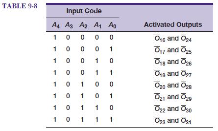
A technician tests the circuit of Figure 9-4 as described in Example 9-7 and finds that the correct output is activated for each possible input code except those listed in Table 9-8. Examine this table and determine the probable cause of the malfunction.Data from Example 9-7A technician tests the
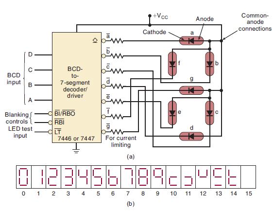
Suppose that a 22-Ω resistor was mistakenly used for the g segment in Figure 9-8. How would this affect the display? What possible problems could occur?Figure 9-8 D C BCD input B Blanking, controls LED test input 0 BCD- to- 7-segment decoder/ driver -BI/RBO RBI LT 2pm 7446 or
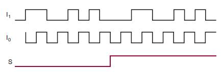
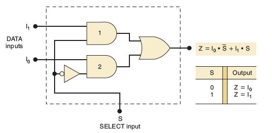
The timing diagram in Figure 9-77 is applied to Figure 9-19. Draw the output waveform Z.Figure 9-77Figure 9-19 S ப பரீ th Tட
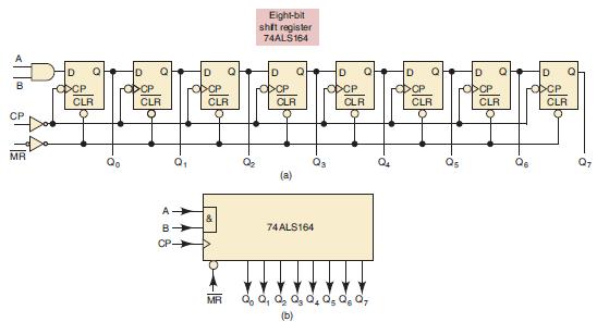
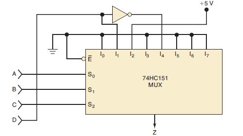
Figure 7-73 shows an eight-bit shift register that could be used to delay a signal by 1 to 8 clock periods. Show how to wire a 74151 to this shift register in order to select the desired Q output and indicate the logic level necessary on the select inputs to provide a delay of 6 × Tclk.Figure 7-73
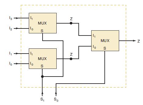
(a) Use the idea from Problem 9-29 to arrange several 74151 1-of-8 multiplexers to form a 1-of-64 multiplexer.(b) Use a Quartus II megafunction to create a 1-of-2 MUX, a 1-of-4 MUX, and a 1-of-8 MUX.Data from Problem 9-29The circuit in Figure 9-78 uses three two-input multiplexers (Figure 9-19).
(a) Show how two 74157s and a 74151 can be arranged to form a 1-of-16 multiplexer with no other required logic. Label the inputs I0 to I15 to show how they correspond to the select code.(b) Create a 1-of-16 multiplexer using a megafunction.
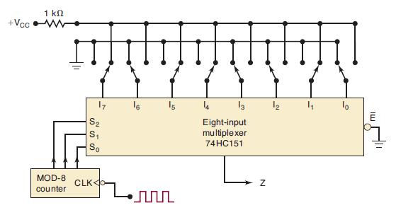
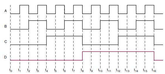
Figure 9-79 shows how a multiplexer can be used to generate logic waveforms with any desirable pattern. The pattern is programmed using eight SPDT switches, and the waveform is repetitively produced by pulsing the MOD-8 counter. Draw the waveform at Z for the given switch positions.Figure 9-79
Change the MOD-8 counter in Figure 9-79 to a MOD-16 counter, and connect the MSB to the multiplexer E̅ input. Draw the Z waveform.Figure 9-79 +Vcc 1 ΚΩ MOD-8 counter 17 S₂ S₁ So CLK- 16 M 14 13 Eight-input multiplexer 74HC151 N l2 lo IW E
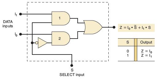
Show how a 74151 can be used to generate the logic function Z = AB + BC + AC.
Show how a 16-input multiplexer such as the 74150 is used to generate the function Z = A B CD + BCD + AB D + ABCD.
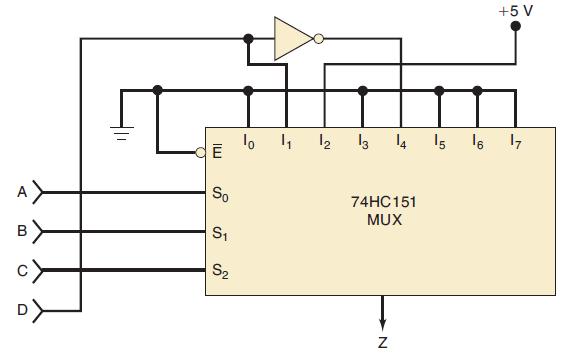
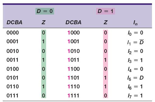
The circuit of Figure 9-80 shows how an eight-input MUX can be used to generate a four-variable logic function, even though the MUX has only three SELECT inputs. Three of the logic variables A, B, and C are connected to the SELECT inputs. The fourth variable D and its inverse D are connected to
The hardware method used in Figure 9-80 can be used to generate any four-variable logic function. For example, is implemented by following these steps:1. Set up a truth table in two halves, side by side as shown in Table 9-9. Notice that the left half shows all combinations of CBA when D = 0, and
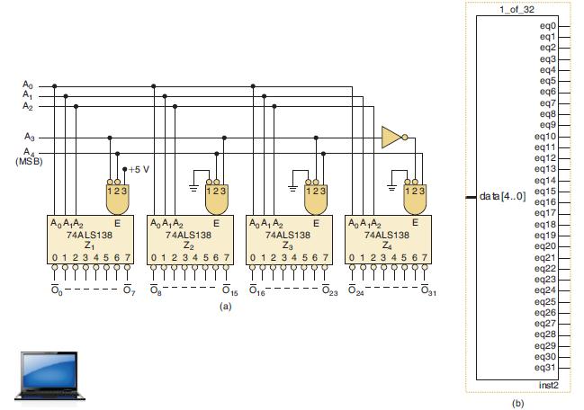
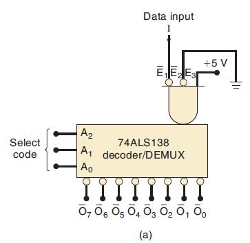
Apply the waveforms of Figure 9-75 to the inputs of the 74ALS138 DEMUX of Figure 9-30(a) as follows:Draw the waveforms at the DEMUX outputs.Fiure 9-75Figure 9-30(a) D→ A₂ C → A₁ B→ Ao A → E₁
For each item, indicate whether it is referring to a decoder, an encoder, a MUX, or a DEMUX.(a) Has more inputs than outputs.(b) Uses SELECT inputs.(c) Can be used in parallel-to-serial conversion.(d) Produces a binary code at its output.(e) Only one of its outputs can be active at one time.(f) Can
Show how the 7442 decoder can be used as 1-to-8 demultiplexer.
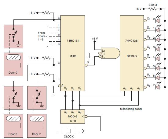
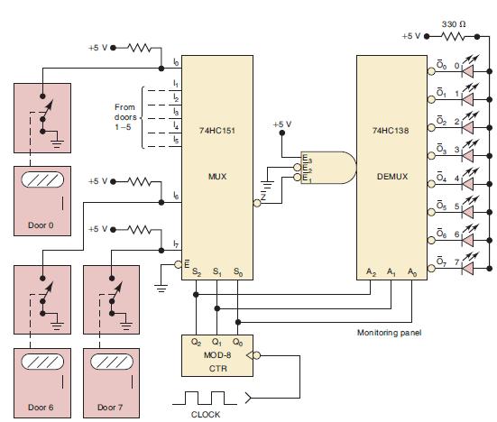
Consider the system of Figure 9-31. Assume that the clock frequency is 10 pps. Describe what the monitoring panel indications will be for each of the following cases.(a) All doors closed (b) All doors open (c) Doors 2 and 6 openFigure 9-31 Door 0 Door 6 +5 V +5 V From doors 1-5 Door
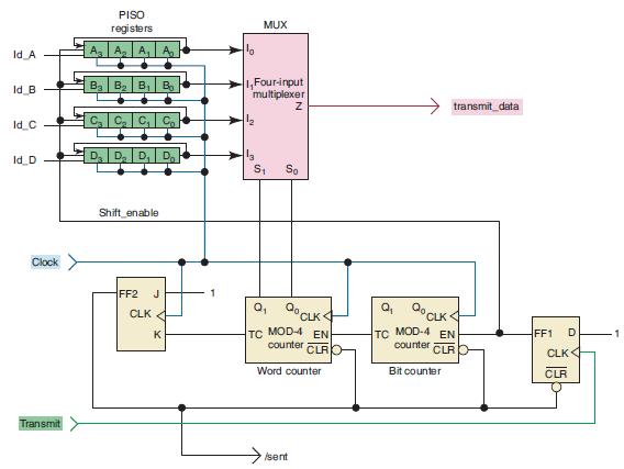
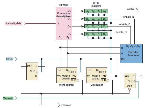
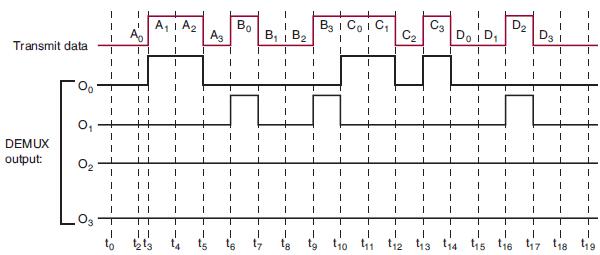
Draw the waveforms at transmit_data, and DEMUX outputs O0, O1, O2, and O3 in Figure 9-33 for the following register data loaded into the transmit registers in Figure 9-32: [A] = 0011, [B] = 0110, [C] = 1001, [D] = 0111.Figure 9-32Figure 9-33 Id
Modify the system of Figure 9-31 to handle 16 doors. Use a 74150 16-input MUX and two 74LS138 DEMUXes. How many lines are going to the remote monitoring panel?Figure 9-31 Door 0 Door 6 +5 V +5 V From doors 1-5 Door 7 1 I I L ||| 4₂ 13 h 7AHC151 MUX Q₂ Q₁ Qo MOD-8 CTR JUL> CLOCK +5 V +5
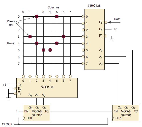
Figure 9-81 shows an 8 × 8 graphic LCD display grid controlled by a 74HC138 configured as a decoder, and a 74HC138 configured as a demultiplexer. Draw 48 cycles of the clock and the data input necessary to activate the pixels shown on the display.Figure 9-81 +5 Pixels on ||| CLOCK O 3 Rows
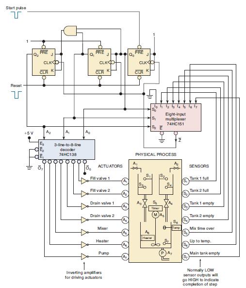
Consider the control sequencer of Figure 9-26. Describe how each of the following faults will affect the operation.(a) The I3 input of the MUX is shorted to ground.(b) The connections from sensors 3 and 4 to the MUX are reversed.Figure 9-26 Start pulse T Reset T Q₂ +5 V PRE CLKO CLA
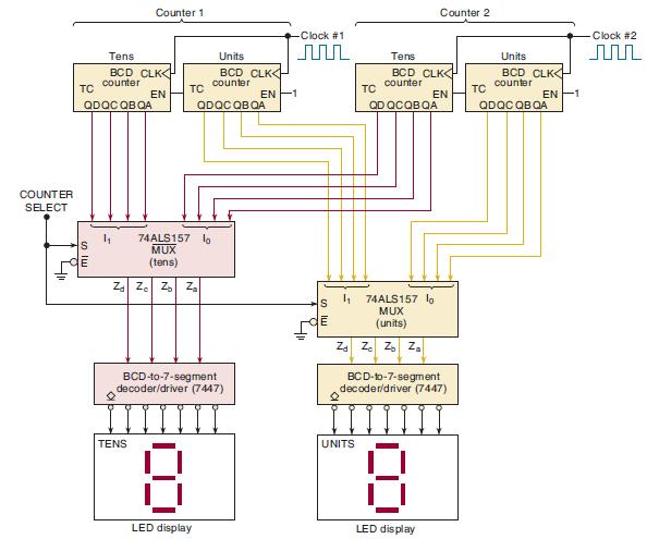
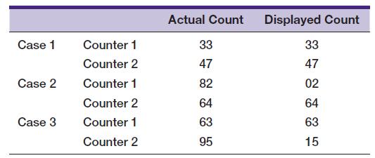
Consider the circuit of Figure 9-24. A test of the circuit yields the results shown in Table 9-10. What are the possible causes of the malfunction?Figure 9-24Table 9-10 COUNTER SELECT TC QDQC QB QA SIE CE Tens BCD CLK counter Counter 1 EN TENS TC 4₁ 74ALS157 lo MUX (tens) Zo Zo Zo Z₂ Units BCD
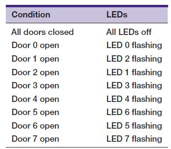
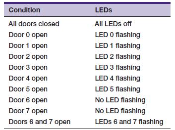
A test of the security monitoring system of Figure 9-31 produces the results recorded in Table 9-11. What are the possible faults that could cause this operation?Table 9-11Figure 9-31 Condition All doors closed Door 0 open Door 1 open Door 2 open Door 3 open Door 4 open Door 5 open Door 6 open Door
The synchronous data transmission system of Figure 9-32 and Figure 9-33 is malfunctioning. An oscilloscope is used to monitor the MUX and DEMUX outputs during the transmission cycle, with the results shown in Figure 9-82. What are the possible causes of the malfunction?Figure 9-82Figure 9-32Figure
A test of the security monitoring system of Figure 9-31 produces the results recorded in Table 9-12. What are the possible faults that could cause this operation? How can this be verified or eliminated as a fault?Table 9-12Figure 9-31 Condition All doors closed Door 0 open Door 1 open Door 2
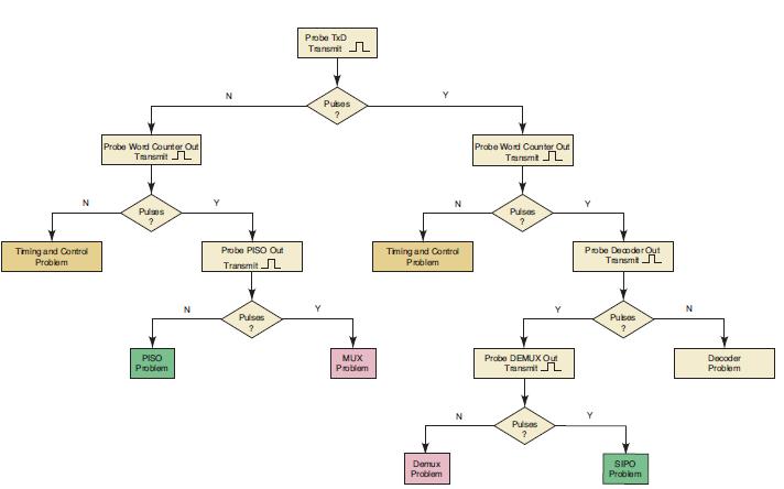
The synchronous data transmission system of Figures 9-32 and 9-33 is not working properly and the troubleshooting tree diagram of Figure 9-38 has been used to isolate the problem to the timing and control section of the receiver. Draw a troubleshooting tree diagram that will isolate the problem
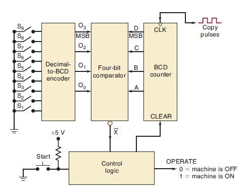
Redesign the circuit of Problem 9-16 using a 74HC85 magnitude comparator. Add a “copy overflow” feature that will activate an ALARM output if the OPERATE output fails to stop the machine when the requested number of copies is done.Data from problem 9-16Figure 9-76 shows the block diagram of a
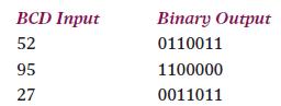
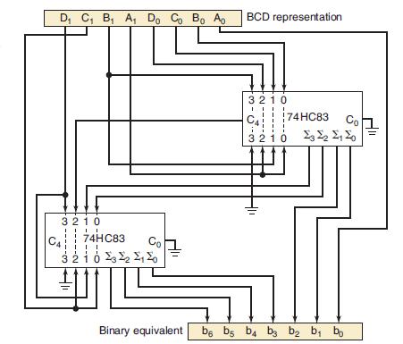
A technician tests the code converter of Figure 9-43 and observes the following results:What is the probable circuit fault?Figure 9-43 BCD Input 52 95 27 Binary Output 0110011 1100000 0011011
Assume a BCD input of 69 to the code converter of Figure 9-43. Determine the levels at each Σ output and at the final binary output.Figure 9-43 D₁ C₁ B₁ A₁ Do Co Bo Ao 3210 !!!! Co 74HC83 3 2 4 6 Σ. Σ. Σ. Σ ! ! ! ! C4 BCD representation 3210 I C 74HC83 Co1 3 2 1 0 ΣΣΣΣ I Binary
(a) Show how to connect 74HC85s to compare two 10-bit numbers.(b) Create a 10-bit comparator using a megafunction.
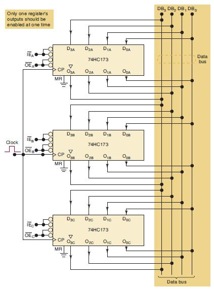
For the bus arrangement of Figure 9-47, describe the input signal requirements for simultaneously transferring the contents of register C to both of the other registers.Figure 9-47 Only one register's outputs should be enabled at one time Clock TEA OEA IE₂ E OEC LITI V CP
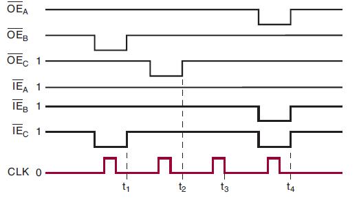
Assume that the registers in Figure 9-47 are initially [A] = 1011, [B] = 1000, and [C] = 0111. The signals in Figure 9-83 are applied to the register inputs.(a) Determine the contents of each register at times t1, t2, t3, and t4.(b) Describe what would happen if I̅E̅A were LOW when the third
True or false:(a) A device connected to a data bus should have tristate outputs.(b) Bus contention occurs when more than one device takes data from the bus.(c) Larger units of data can be transferred over an eight-line data bus than over a four-line data bus.(d) A bus driver IC generally has a high
Assume the same initial conditions of Problem 9-58, and sketch the signal on DB3 for the waveforms of Figure 9-83.Data from Problem 9-58Assume that the registers in Figure 9-47 are initially [A] = 1011, [B] = 1000, and [C] = 0111. The signals in Figure 9-83 are applied to the register
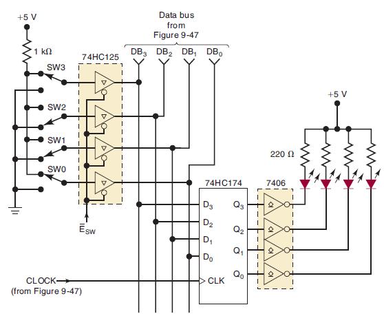
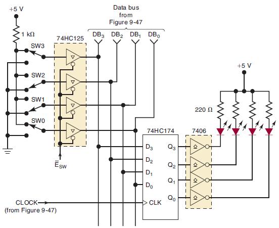
Figure 9-84 shows two more devices that are to be added to the data bus of Figure 9-47. One is a set of buffered switches that can be used to enter data manually into any of the bus registers. The other device is an output register that is used to latch any data that are on the bus during a data
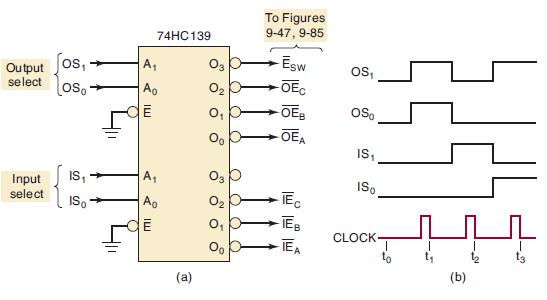
Now that the circuitry of Figure 9-85 has been added to Figure 9-47, a total of five devices are connected to the data bus. The circuit in Figure 9-85(a) will now be used to generate the enable signals needed to perform the different data transfers over the data bus. It uses a 74HC139 chip that
Show how a 74HC541 (Figure 9-50) can be used in the circuit of Figure 9-84.Figure 9-84Figure 9-50 +5 V 1 ΚΩ SW3 SW2 SW1 SWO 74HC125 CLOCK- (from Figure 9-47) 1 1 Data bus from Figure 9-47 DB 3 DB₂ DB, DB 74HC174 D3 Q3 D₂ D₁ Do CLK Q₂ Q₁ Qo I 1 1 220 Ω 7406 2 a K e +5 V ww ww
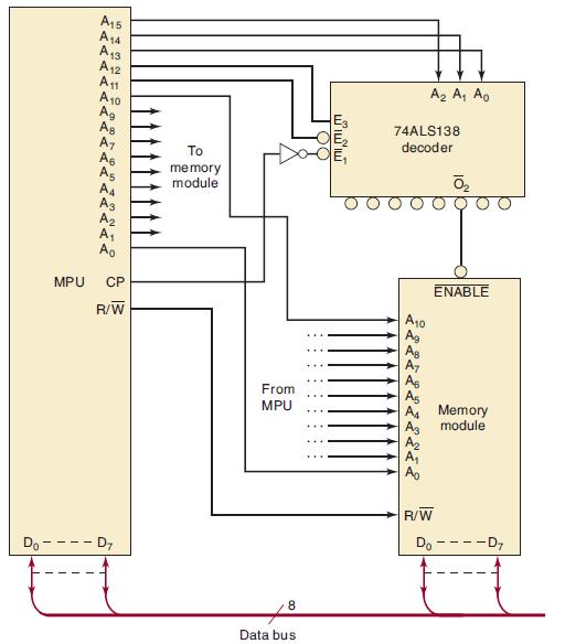
Figure 9-86 shows the basic circuitry to interface a microprocessor (MPU) to a memory module. The memory module will contain one or more memory ICs (Chapter 12) that can either receive data from the MPU (a WRITE operation) or send data to the MPU (a READ operation). The data are transferred over
The keyboard entry circuit of Figure 9-16 is to be used as part of an electronic digital lock that operates as follows: when activated, an UNLOCK output goes HIGH. This HIGH is used to energize a solenoid that retracts a bolt and allows a door to be opened. To activate UNLOCK, the operator must
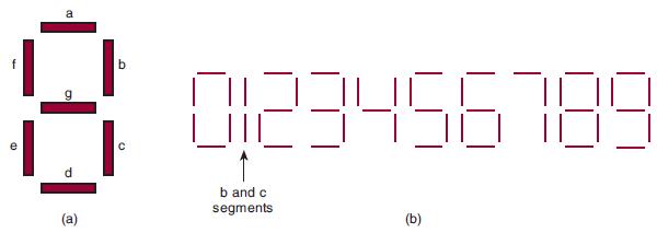
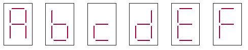
Write the HDL code for a hex decoder/driver for a 7-segment display. The first 10 characters should appear as shown in Figure 9-7. The last six characters should appear as shown in Figure 9-87.Figure 9-7Figure 9-87 e a P (a) b C 23456789 IO b and c segments (b)
Write the HDL code for a BCD-to-decimal decoder (the equivalent of a 7442).
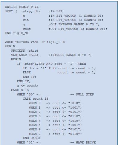
Modify the stepper design file of Figure 10-8 or 10-9 to add an enable input that puts the outputs in the Hi-Z state (tristate) when enable = 0.Figure 10-8Figure 10-9 SUBDESIGN [ig10 8. ( ) step, dir m[1..0), cin 13..01 cout [3..0]. q[2..0] VARIABLE count [2..0] BEGIN DFF; count().clk step; IF dir
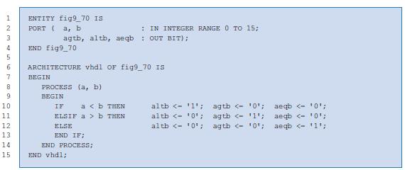
Use HDL to describe a three-digit BCD code to eight-bit binary number converter. (Maximum BCD input is 255.)Figure 9-69Figure 9-70 THEODORUAWNE 7 9 10 11 SUBDESIGN fig9_69 ( a[3..0], b[3..0] agtb, altb, aeqb. > BEGIN IF : INPUT; : OUTPUT; a[] > b[] THEN ELSE END IF; 12 13. END; ELSIF a[]
Write a low-priority ENCODER description that will always encode the lowest number if two inputs are activated simultaneously.
Rewrite the stepper driver design file of Figure 10-8 or 10-9 without using a CASE statement. Use your favorite HDL.Figure 10-8Figure 10-9 SUBDESIGN [ig10 8. ( ) step, dir m[1..0), cin 13..01 cout [3..0]. q[2..0] VARIABLE count [2..0] BEGIN DFF; count().clk step; IF dir THEN
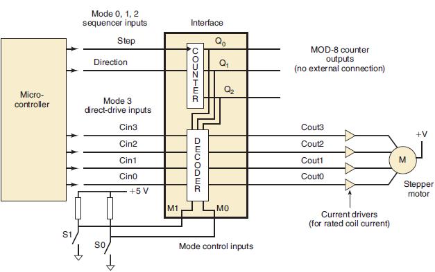
The cout lines of Figure 10-1 started at 1010 and have just progressed through the following sequence: 1010, 1001, 0101, 0110.(a) How many degrees has the shaft rotated?(b) What sequence will reverse the rotation and return the shaft to its original position?Figure 10-1 Micro- controller S1 Mode 0,
Use HDL to describe a four-bit binary number to a two-digit BCD code converter.
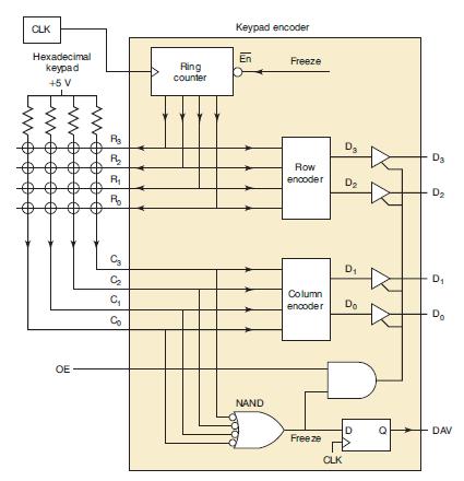
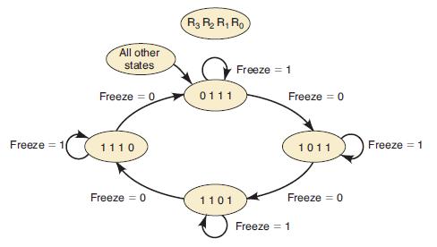
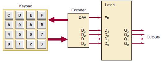
Write the state table for the ring counter shown in Figure 10-11 and described in Figure 10-13.Figure 10-11Figure 10-13 CLK Hexadecimal keypad +5 V wwwww DA DO $0 $ OE PPPP R₂ R₂ P₂ C₂ C₂ $ 5 Co Ring counter Keypad encoder En NAND Freeze Row encoder
Describe a method to test the stepper driver in:(a) Full-step mode(b) Half-step mode(c) Wave-drive mode(d) Direct-drive mode
With no keys pressed, what is the value on c[3..0]?
Assume that the ring counter is in state 0111 when someone presses the 7 key. Will the ring counter advance to the NEXT state?
Assume the 9 key is pressed and held until DAV = 1.(a) What is the value on the ring counter?(b) What is the value encoded by the row encoder?(c) What is the value encoded by the column encoder?(d) What binary number is on the D[3..0] lines?
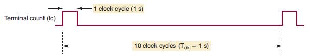
Assume a 1-Hz clock is applied to the seconds stage of the clock in Figure 10-17. The MOD-10 units of seconds counter’s terminal count (tc) output is shown in Figure 10-51. Draw a similar diagram showing the number of clock cycles between the tc output pulses of each of the following:(a) Tens of
In Problem 10-12, will the data be valid on the falling edge of DAV?Data from Problem 10-12Assume the 9 key is pressed and held until DAV = 1.What is the value on the ring counter?What is the value encoded by the row encoder?What is the value encoded by the column encoder?What binary number is on
The keypad is connected to a 74373 octal transparent latch as shown in Figure 10-50. The output is correct as long as a key is held. However, it is unable to latch data between key presses. Why will this circuit not work correctly?Figure 10-50 Keypad C D E F CO 9 5 0 1 A
How many cycles of the 60-Hz power line will occur in a 24-hour period? What problem do you think will result if we attempt to simulate the operation of the entire clock circuit?
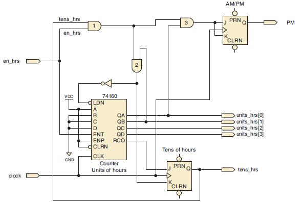
Modify the hours stage of Figure 10-18 to keep military time (00–23 hours).Figure 10-18 en_hrs clock tens hrs en_hrs VCC GND 1 74160 LDN A B с D ENT ENP CLRN CLK QA QB QC QD RCO Counter Units of hours 3 Tens of hours 6 PRN KCLRN AMPM K PRN CLRN units_hrs[0] units_hrs [1] units_hrs
Refer to Figure 10-42. Each counter block in this figure represents the lowest level of the hierarchy established for this project: a primary functional block. Its specifications are MOD 10 (or 6), BCD down counter, active-LOW synchronous load, active-LOW asynchronous clear, active-HIGH enable,
Many digital clocks are set by simply making them count faster while a push button is held down. Modify the design to add this feature.
Refer to Figure 10-43. The sub-blocks (encoder, divide-by counter, non-recycling counter, MUX) could be implemented as separate blocks in the third level of hierarchy of this project. Code can be found in previous examples that will work for each of these blocks with only slight modification. These
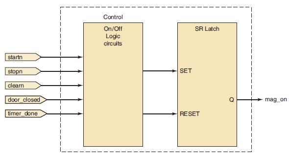
Refer to Figure 10-44. The block on the left is simply combinational logic that must control the S-R latch that turns on and off the magnetron tube.(a) Draw a logic diagram using only gates to implement this circuit.(b) Describe this block using AHDL.(c) Describe this block using VHDL.Figure 10-44
Refer to Figure 10-45. This block decodes the three BCD digits from the timer block and drives the active-LOW 7-segment LED displays. It must also accomplish leading zero blanking.(a) Use 7447 standard logic blocks to implement this block.(b) Use AHDL to implement this block.(c) Use VHDL to
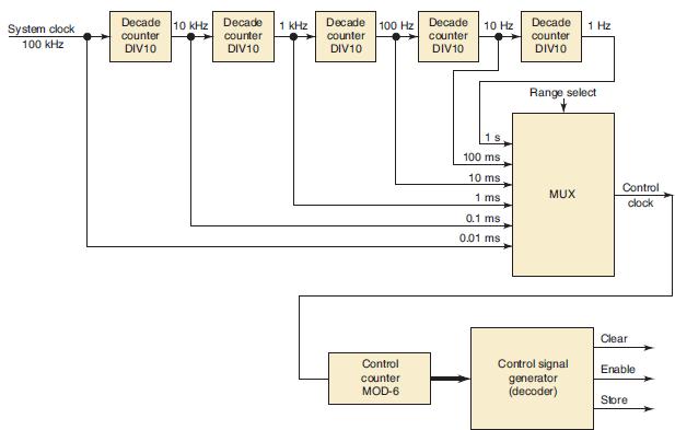
Write the HDL code for the MOD-6 control counter and control signal generator in Figure 10-49.Figure 10-49 System clock 100 kHz Decade 10 kHz Decade counter counter DIV10 DIV10 1 kHz Decade 100 Hz counter DIV10 Control counter MOD-6 Decade counter DIV10 10 Hz 100 ms 10 ms 1 ms 0.1 ms 0.01
Draw the hierarchy diagram for the frequency counter project.
Write the HDL code for the MUX of Figure 10-49.Figure 10-49 System clock 100 kHz Decade 10 kHz Decade counter counter DIV10 DIV10 1 kHz Decade 100 Hz counter DIV10 Control counter MOD-6 Decade counter DIV10 10 Hz 100 ms 10 ms 1 ms 0.1 ms 0.01 ms Decade counter DIV10 Range select MUX 1 Hz Control
Use graphic design techniques and the BCD counter described in Figure 10-31, the MUX, and the control signal generator design to create the entire timing and control block for the frequency counter project.Figure 10-31 FIG10_24 CLOCK Q[2..0] ENABLE TC MOD-6 from VHDL (a) FIG10_26 CLOCK
Write the HDL code for the timing and control section of the frequency counter.
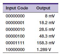
A certain DAC has the following specifications: eight-bit resolution, full scale = 2.55 V, offset ≤ 2 mV; accuracy = ±0.1% F.S. A static test on this DAC produces the results shown in Table 11-11. What is the probable cause of the malfunction?Table 11-11 Input
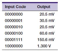
Repeat Problem 11-20 using the measured data given in Table 11-12.Table 11-12Data from Problem 11-20A certain DAC has the following specifications: eight-bit resolution, full scale = 2.55 V, offset ≤ 2 mV; accuracy = ±0.1% F.S. A static test on this DAC produces the results shown in Table 11-11.
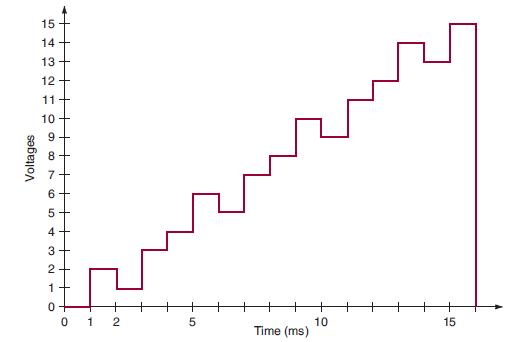
A technician connects a counter to the DAC of Figure 11-3 to perform a staircase test using a 1-kHz clock. The result is shown in Figure 11-36. What is the probable cause of the incorrect staircase signal?Figure 11-36Figure 11-3 Voltages 15 14 13 11- 10 00 N 6 5 2 0 0 T 2 5 Time (ms) 10 15
Fill in the blanks in the following description of the ADC of Figure 11-13. Each blank may be one or more words.A START pulse is applied to _______________ the counter and to keep _______________ from passing through the AND gate into the _______________. At this point, the DAC output, VAX, is
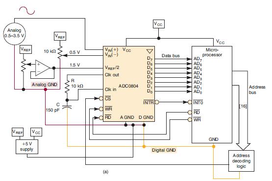
Connect a 2.0-V reference source to VREF/2, and repeat Problem 11-38.Data from Problem 11-38Refer to Figure 11-21. What is the approximate value of the analog input if the microcomputer’s data bus is at 10010111 when R̅D̅ is pulsed LOW?Figure 11-21 Analog 0.5-3.5 V VREF IN REF Voc VREF Analog
Refer to Figure 11-21. What is the approximate value of the analog input if the microcomputer’s data bus is at 10010111 when R̅D̅ is pulsed LOW?Figure 11-21 Analog 0.5-3.5 V VREF IN REF Voc VREF Analog GND +5V supply 10 ΚΩ C 150 pF 매 0.5 V 1.5 V R 10 ΚΩ VIN(+) Voc V₁(-) VREF/2 Cik
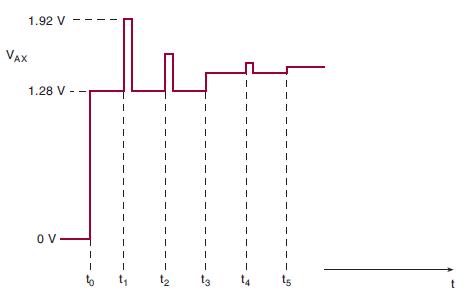
Figure 11-39 shows the waveform at VAX for a six-bit SAC with a step size of 40 mV during a complete conversion cycle. Examine this waveform and describe what is occurring at times t0 to t5. Then determine the resultant digital output.Figure 11-39 1.92 V VAX 1.28 V- OV- 1 I to t₁ 1₂ 1 14 1 15 t
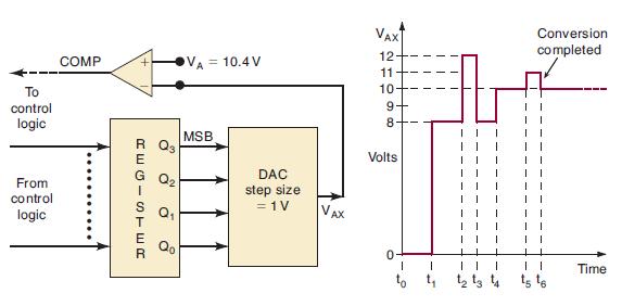
Repeat Problem 11-34 for VA = 16 V.Data from Problem 11-34Draw the waveform for VAX as the SAC of Figure 11-19 converts VA = 6.7 V.Figure 11-19 To control logic From control logic COMP REGISTER R Q3 G Q₂ o VA = 10.4 V MSB DAC step size = 1V VAX VAX 12 11 10+ 9+ 8 Volts 0 I to I I II 1 t₁ IL +
Draw the waveform for VAX as the SAC of Figure 11-19 converts VA = 6.7 V.Figure 11-19 To control logic From control logic COMP REGISTER R Q3 G Q₂ o VA = 10.4 V MSB DAC step size = 1V VAX VAX 12 11 10+ 9+ 8 Volts 0 I to I I II 1 t₁ IL + + 1 1₂ 13 14 Conversion completed 11 15 16 Time
An eight-bit digital-ramp ADC with a 40-mV resolution uses a clock frequency of 2.5 MHz and a comparator with VT = 1 mV. Determine the following values.(a) The digital output for VA = 6.000 V(b) The digital output for 6.035 V(c) The maximum and average conversion times for this ADC
Why were the digital outputs the same for parts (a) and (b) of Problem 11-24?Data from Problem 11-24An eight-bit digital-ramp ADC with a 40-mV resolution uses a clock frequency of 2.5 MHz and a comparator with VT = 1 mV. Determine the following values.(a) The digital output for VA = 6.000 V(b) The
What would happen in the ADC of Problem 11-24 if an analog voltage of VA = 10.853 V were applied to the input? What waveform would appear at the D/A output? Incorporate the necessary logic in this ADC so that an “overscale” indication will be generated whenever VA is too large.Data from Problem
An ADC has the following characteristics: resolution, 12 bits; fullscale error, 0.03% F.S.; full-scale output, +5 V.(a) What is the quantization error in volts?(b) What is the total possible error in volts?
The quantization error of an ADC such as the one in Figure 11-13 is always positive because the VAX value must exceed VA in order for the comparator output to switch states. This means that the value of VAX could be as much as 1 LSB greater than VA. This quantization error can be modified so that
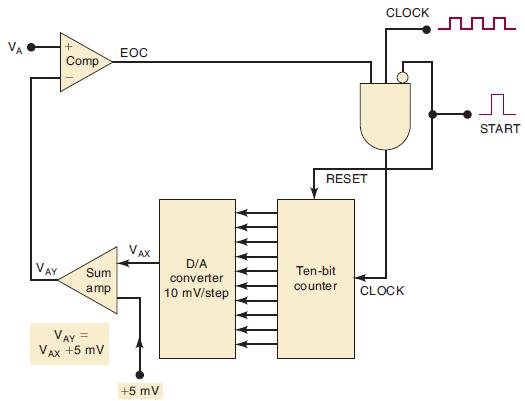
For the ADC of Figure 11-37, determine the range of analog input values that will produce a digital output of 0100011100.Figure 11-37 VAY Comp Sum amp VAY = VAX +5 mV EOC VAX +5 mV D/A converter 10 mV/step RESET Ten-bit counter CLOCK CLOCK START
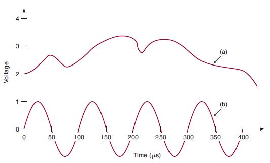
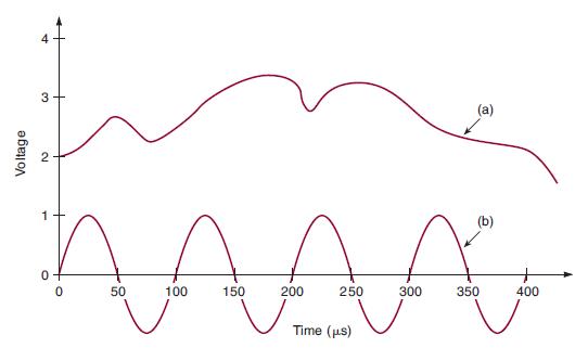
Assume that the analog signal in Figure 11-38(a) is to be digitized by performing continuous A/D conversions using an eight-bit digital ramp converter whose staircase rises at the rate of 1 V every 25 μs. Sketch the reconstructed signal using the data obtained during the digitizing process.
On the sine wave of Figure 11-38(b), mark the points where samples are taken by a flash A/D converter at intervals of 75 μs (starting at the origin). Then draw the reconstructed output from the D/A converter (connect the sample points with straight lines to show filtering). Calculate the sample
A sampled data acquisition system is being used to digitize an audio signal. Assume the sample frequency FS is 20 kHz. Determine the output frequency that will be heard for each of the following input frequencies.(a)*Input signal = 5 kHz(b)*Input signal = 10.1 kHz(c) Input signal = 10.2 kHz(d)
Indicate whether each of the following statements refers to the digitalramp ADC, the successive-approximation ADC, or both.(a) Produces a staircase signal at its DAC output(b) Has a constant conversion time independent of VA(c) Has a shorter average conversion time(d) Uses an analog comparator(e)
A certain eight-bit successive-approximation converter has 2.55 V full scale. The conversion time for VA = 1 V is 80 μs. What will be the conversion time for VA = 1.5 V?
Discuss how a flash ADC with a conversion time of 1 μs would work for the situation of Problem 11-30.Data from Problem 11-30Assume that the analog signal in Figure 11-38(a) is to be digitized by performing continuous A/D conversions using an eight-bit digital ramp converter whose staircase rises
For each of the following statements, indicate which type of ADC— digital-ramp, SAC, or flash—is being described.(a) Fastest method of conversion(b) Needs a START pulse(c) Requires the most circuitry(d) Does not use a DAC(e) Generates a staircase signal(f) Uses an analog comparator(g) Has a
For each statement, indicate what type(s) of ADC is (are) being described.(a) Uses subranging stages(b) Uses a large number of comparators(c) Uses a VCO(d) Is used in noisy industrial environments(e) Uses a capacitor(f) Is relatively insensitive to temperature
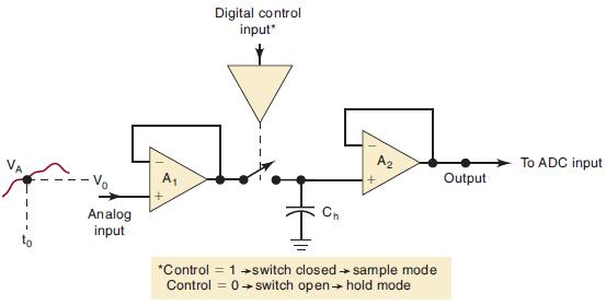
Refer to the S/H circuit of Figure 11-26. What circuit fault would result in VOUT looking exactly like VA? What fault would cause VOUT to be stuck at 0?Figure 11-26 Analog input Digital control input* Ch A₂ *Control = 1 switch closed → sample mode switch open→ hold mode Control = 0 Output To
Use the CMOS 4016 IC to implement the switching in Figure 11-27, and design the necessary control logic so that each analog input is converted to its digital equivalent in sequence. The ADC is a 10-bit, successive-approximation type using a 50-kHz clock signal, and it requires a 10-μs-duration
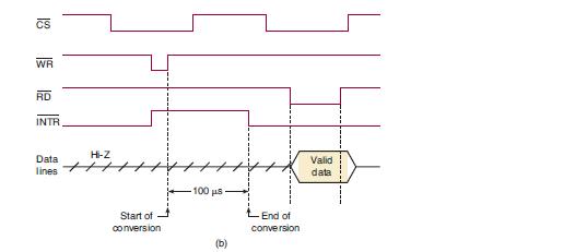
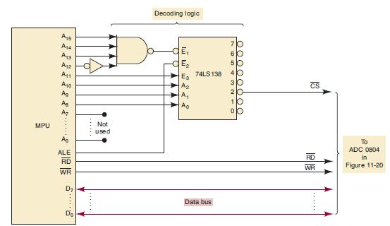
Figure 11-21 shows how the ADC0804 is interfaced to a microcomputer. It shows three control signals, C̅S̅, R̅D̅, and W̅R̅, that come from the microcomputer to the ADC. These signals are used to start each new A/D conversion and to read (transfer) the ADC data output into the microcomputer
You have available a 10-bit SAC A/D converter (AD 573), but your system requires only eight bits of resolution and you have only eight port bits available on your microprocessor. Can you use this A/D converter, and if so, which of the 10 data lines will you attach to the port?
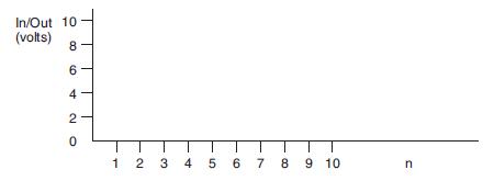
The data in Table 11-13 are input samples taken by an A/D converter. Notice that if the input data were plotted, it would represent a simple step function like the rising edge of a digital signal. Calculate the simple average of the four most recent data points, starting with OUT[4] and proceeding
Showing 300 - 400
of 1612
1
2
3
4
5
6
7
8
9
10
11
12
13
14
15
Last
Step by Step Answers
![SUBDESIGN [ig10 8. ( ) step, dir m[1..0), cin 13..01 cout [3..0]. q[2..0] VARIABLE count [2..0] BEGIN DFF;](https://dsd5zvtm8ll6.cloudfront.net/images/question_images/1700/1/1/8/1246555be6c7c5ea1700118124088.jpg)
![WHEN 2 > END; CASE count[] IS WHEN BROOD" -HALF STEP B1010"; B"1000"; -> cout [] ->cout [1] -> cout [] ->](https://dsd5zvtm8ll6.cloudfront.net/images/question_images/1700/1/1/8/1436555be7f2d7541700118142731.jpg)
![HEMAFETOHEM 1 2 3 4 5 6 7 8 9 10 11 12 SUBDESIGN fig9_69 ( a[3..0], b[3..0] agtb, altb, aeqb. > BEGIN IF a[]](https://dsd5zvtm8ll6.cloudfront.net/images/question_images/1700/1/1/5/3006555b36464b0e1700115300027.jpg)

![data[3.0] C loadn D cim clock enable INPUT Voc INPUT VOC INPUT VOC INPUT VOC D DUNPUT VOC Units of Seconds](https://dsd5zvtm8ll6.cloudfront.net/images/question_images/1700/1/1/8/6946555c0a617e171700118693572.jpg)
![keypad[9..0] enablen 100 Hz clock Priority encoder Enablen BCD out Data valid Divide by 100 (4 Encoder](https://dsd5zvtm8ll6.cloudfront.net/images/question_images/1700/1/1/8/8526555c144e62c51700118852459.jpg)
![keypad (9..0] dock 100 Hz startn stopn clearn door closed INPUT: INPUT INPUT INPUT INPUT INPUT encoder](https://dsd5zvtm8ll6.cloudfront.net/images/question_images/1700/1/1/8/7866555c102b2eff1700118786238.jpg)
![FIG10_24 CLOCK Q[2..0] ENABLE TC MOD-6 from VHDL (a) FIG10_26 CLOCK Q[3..0] ENABLE TC MOD-10 from AHDL (b)](https://dsd5zvtm8ll6.cloudfront.net/images/question_images/1700/1/1/9/0176555c1e9ddcae1700119017439.jpg)
![(IN[n OUT[n] OUT[4] (IN[1] OUT[5] = (IN[2] = - - 3] + IN[n 2] + IN[n + IN[2] + IN[3] + IN[3] + IN[4] 1] +](https://dsd5zvtm8ll6.cloudfront.net/images/question_images/1700/2/0/3/77165570cfb7aedb1700203772653.jpg)
![Sample n IN[n] (V) OUT[n] (V) 1 0 0 2 0 0 3 0 0 4 0 5 10 6 10 7 10 8 10 9 10 10 10](https://dsd5zvtm8ll6.cloudfront.net/images/question_images/1700/2/0/3/61665570c60400201700203617527.jpg)