New Semester
Started
Get
50% OFF
Study Help!
--h --m --s
Claim Now
Question Answers
Textbooks
Find textbooks, questions and answers
Oops, something went wrong!
Change your search query and then try again
S
Books
FREE
Study Help
Expert Questions
Accounting
General Management
Mathematics
Finance
Organizational Behaviour
Law
Physics
Operating System
Management Leadership
Sociology
Programming
Marketing
Database
Computer Network
Economics
Textbooks Solutions
Accounting
Managerial Accounting
Management Leadership
Cost Accounting
Statistics
Business Law
Corporate Finance
Finance
Economics
Auditing
Tutors
Online Tutors
Find a Tutor
Hire a Tutor
Become a Tutor
AI Tutor
AI Study Planner
NEW
Sell Books
Search
Search
Sign In
Register
study help
computer science
digital systems principles and application
Digital Systems Principles And Application 12th Edition Ronald Tocci, Neal Widmer, Gregory Moss - Solutions
Repeat the previous problem using a weighted average of the last four samples. The weights in this case are placing greater emphasis on recent samples and less emphasis on older samples. Use the weights 0.1, 0.2, 0.3, and 0.4.Data from Previous ProblemThe data in Table 11-13 are input samples taken
What does the term MAC stand for?
Design the ADC interface to a digital thermostat using an LM34 temperature sensor and the ADC0804. Your system must measure accurately (±0.2°F) from 50 to 101°F. The LM34 puts out 0.01 V per degree F(0°F = 0°V).(a) What should the digital value for 50°F be for the best resolution?(b) What
True or false:(a) A digital signal is a continuously changing voltage.(b) A digital signal is a sequence of numbers that represent an analog signal. When processing an analog signal, the output may be distorted due to: (a) Quantization error when converting analog to digital (b) Not sampling the
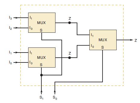
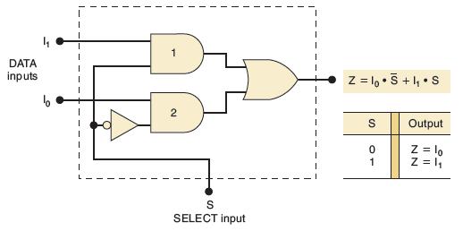
The circuit in Figure 9-78 uses three two-input multiplexers (Figure 9-19). Determine the function performed by this circuit.Figure 9-78Figure 9-19 13 12 lo 4₁ lo 4₁ lo MUX S MUX S S₁ So N N 1₁ 10 MUX S N
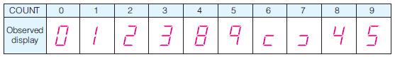
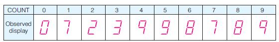
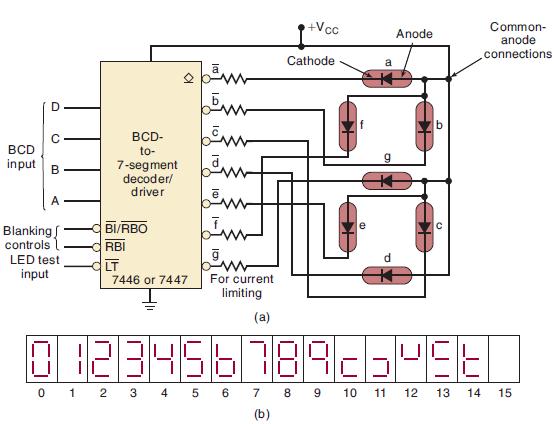
Repeat Example 9-8 with the observed sequence shown below:Data from Example 9-8A technician wires the outputs from a BCD counter to the inputs of the decoder/driver of Figure 9-8. He applies pulses to the counter at a very slow rate and observes the LED display, which is shown below, as the counter
Repeat Example 9-8 with the observed sequence shown below:Data from Example 9-8A technician wires the outputs from a BCD counter to the inputs of the decoder/driver of Figure 9-8. He applies pulses to the counter at a very slow rate and observes the LED display, which is shown below, as the counter
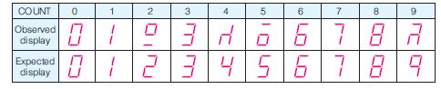
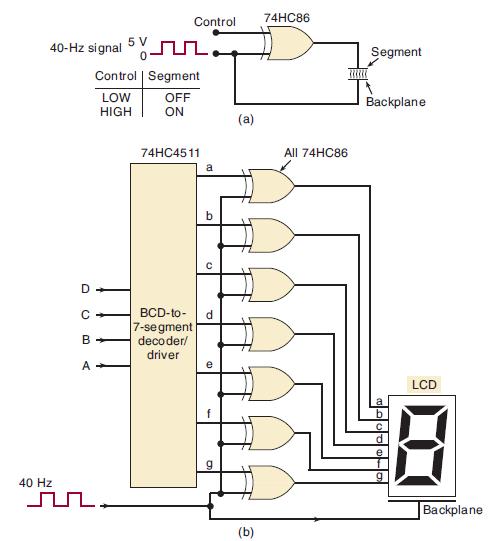
To test the circuit of Figure 9-10, a technician connects a BCD counter to the 74HC4511 inputs and pulses the counter at a very slow rate. She notices that the f segment works erratically, and no particular pattern is evident. What are some of the possible causes of the malfunction?Figure 9-10
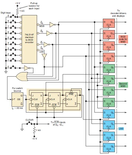
While testing the circuit of Figure 9-16, a technician finds that every odd-numbered key results in the correct digit being entered, but every even-numbered key results in the wrong digit being entered as follows: the 0 key causes a 1 to be entered, the 2 key causes a 3 to be entered, the 4 key
For a 74ALS173,(a) What input conditions will produce the load operation?(b) What input conditions will produce the hold operation?(c) What input conditions will allow the internal register outputs to appear at O0 to O3?
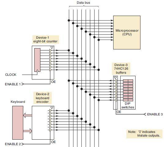
(a) For Figure 9-44, describe the conditions necessary to transmit data from device 3 to the microprocessor.(b) What will the status of the data bus be when none of the devices is enabled?Figure 9-44 CLOCK ENABLE 1 Keyboard ENABLE 2> Device-1 eight-bit
Repeat Problem 9-18 with the following symptom: the registers and displays stay at 0 no matter how many times a key is pressed.Data from Problem 9-18A technician breadboards the keyboard entry circuit of Figure 9-16 and tests its operation by trying to enter a series of three-digit numbers. He
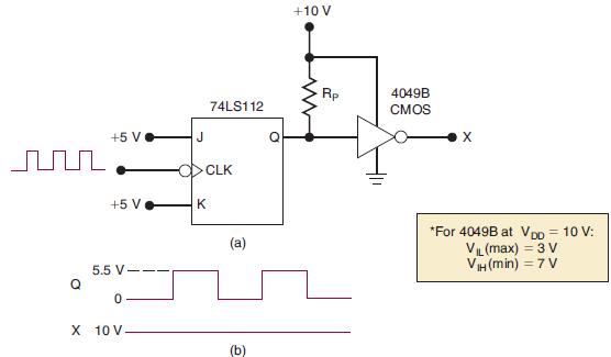
Refer to Figure 8-65(a), where a 74LS TTL output, Q, is driving a CMOS INVERTER operating at VDD = 10 V. The waveforms at Q and X appear as shown in Figure 8-65(b). Which of the following is a possible reason why X stays HIGH?(a) The 10-V supply is faulty.(b) The pull-up resistor is too large.(c)
The circuit of Figure 8-50 has a solder bridge to ground somewhere between the output of the NAND gate and the input of the FF. Describe a procedure for a test that could be performed to indicate that the fault is on the circuit board and probably not in either the NAND or the FF ICs.Figure 8-50
In Figure 8-44, a logic probe indicates that the lower end of the pull-up resistor is stuck in the LOW state. Which of the following is the possible fault?(a) The TTL gate’s current-sourcing transistor is open.(b) The TTL gate’s current-sinking transistor has a collector–emitter short.(c)
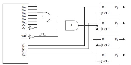
In Chapter 5, we saw how a microprocessor (MPU), under software control, transfers data to an external register. The circuit diagram is repeated in Figure 8-69. Once the data are in the register, they are stored there and used for whatever purpose they are needed. Sometimes, each individual bit in
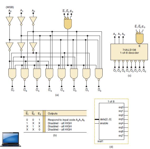
Refer to Figure 9-3. Determine the levels at each decoder output for the following sets of input conditions.(a) All inputs LOW(b) All inputs LOW except E3 = HIGH(c) All inputs HIGH except E̅1 = E̅2 = LOW(d) All inputs HIGHFigure 9-3 (MSB) A₂ 10 lo Ao OTX E₁ E₂ E OxrX 0 0 Ō₁ 1 OXXL X X X
Indicate the states of the 74ALS138 outputs for each of the following sets of inputs. (a) E3 = E₂ = 1, E₁ = 0, A₂ = A₁ = 1, 40 = 0 = E₁ = 0, A₂ = 0, A₁ = 40 = 1 (b) E3 = 1, E₂
Can more than one decoder output be activated at one time?
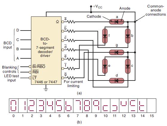
Which LED segments will be on for a decoder/driver input of 1001?
Indicate which of the following statements refer to LCD displays and which refer to LED displays.(a) Emit light(b) Reflect ambient light(c) Are best for low-power applications(d) Require an AC voltage(e) Use a 7-segment arrangement to produce digits(f) Require current-limiting resistors
How does an encoder differ from a decoder?
Name the two troubleshooting techniques described in this section.
What is the function of a multiplexer’s select inputs?
What are some of the major applications of multiplexers?
Explain the difference between a DEMUX and a MUX.
What is the purpose of the cascading inputs of the 74HC85?
What is a code converter?
What is meant by the term data bus?
What will happen if O̅E̅A = O̅E̅B = LOW in Figure 9-47?Figure 9-47 Only one register's outputs should be enabled at one time Clock TEA OE IE₂ g OE TEC W OEC 0000 II V CP 03A MR CP MR D₂A MR D₂A CP 030 74HC173 DIA DOA 0₂A O1A D₂8 D₂8 D₁8 74HC173 0₂8 Dac
Assume that both I̅E̅ inputs are LOW and that D0D1D2D3 = 1011. What logic levels are present at the FF D inputs?
What is the purpose of the 74138’s three inputs e3, e2bar, and e1bar?
What feature of a 7447 is very difficult to duplicate in PLD hardware and HDL code?
Name two methods in AHDL for giving priority to some inputs over others.
For the four-bit by four-channel MUX, name the data inputs, the dataoutputs, and the control inputs that choose one channel of the four.
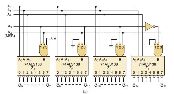
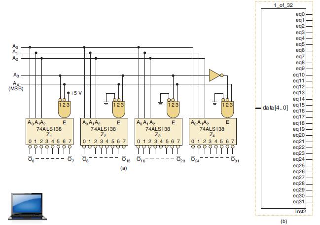
Figure 9-4(a) shows how four 74ALS138s and an INVERTER can be arranged to function as a 1-of-32 decoder. The decoders are labeled Z1 to Z4 for easy reference, and the eight outputs from each one are combined into 32 outputs. Z1’s outputs are O̅0 to O̅7; Z2’s outputs O̅0 to O̅7 are renamed
What type of data objects must be declared for data inputs to a comparator?
For a two-digit BCD (eight-bit) number, what is the decimal weight of the most significant digit?
What is the number of inputs and outputs of a decoder that accepts 64 different input combinations?
What is the function of a decoder’s enable input(s)?
True or false: More than one output of a BCD-to-7-segment decoder/drivercan be active at one time.
What form of data is sent to each of the following?(a) A 7-segment LCD display with a decoder/driver(b) An alphanumeric LCD module(c) An LCD computer display
How does a priority encoder differ from an ordinary encoder?
In the first technique, describe what is observed and what is beinganalyzed.
A certain multiplexer can switch one of 32 data inputs to its output. Howmany different inputs does this MUX have?
True or false: When a multiplexer is used to implement a logic function,the logic variables are applied to the multiplexer’s data inputs.
True or false: The circuit for a DEMUX is basically the same as for a decoder.
What are the outputs of a 74HC85 with the following inputs: A3A2A1A0 = B3B2B1B0 = 1001, IA>B = IA = 0, and IA=B = 1?
How many binary outputs would a three-digit BCD-to-binary converter have?
What is bus contention, and what must be done to prevent it?
True or false: The register cannot be loaded when the master reset input (MR) is held HIGH.
What logic level is on a data bus line when all devices tied to the bus are disabled?
Name two AHDL methods to describe a decoder’s operation.
Are the HDL decoder driver examples intended to drive common-anode or common-cathode 7-segment displays?
Name two methods in VHDL for giving priority to some inputs overothers.
For the four-bit by four-channel DEMUX, name the data inputs, thedata outputs, and the control inputs that choose one channel of the four.
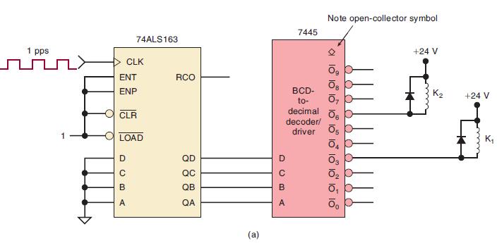
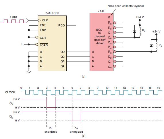
Describe the operation of the circuit in Figure 9-6(a).Figure 9-6(a). 1 pps 74ALS163 CLK ENT ENP CLR DCBA LOAD RCO QD QC QB QA (a) 7445 C B A BCD- to- decimal decoder/ driver Note open-collector symbol ōg Ōg Ō, Ō6 10 10 10 10 10 10 03 +24 V +24 V K₁
What is the key control structure used to describe a comparator?
In AHDL, how is multiplication by 10 accomplished?
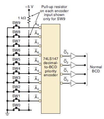
What will the outputs be in Figure 9-15 when SW6, SW5, and SW2 are all closed?Figure 9-15 1 ΚΩ SW9 SW8 SW7 SW6 SW5 SW4 SW3 SW2 SW1 SWO +5 V As Āg Ā₁ Ā6 Pull-up resistor on each encoder input shown only for SW9 74LS147 As decimal- Ā4 to-BCD priority encoder ।द Ā₂ Ã₁ YYYY 5] ]]
For a 74ALS138, what input conditions will produce the following outputs:(a) LOW at O̅6(b) LOW at O̅3(c) LOW at O̅5(d) LOW at O̅0 and O̅7, simultaneously
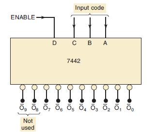
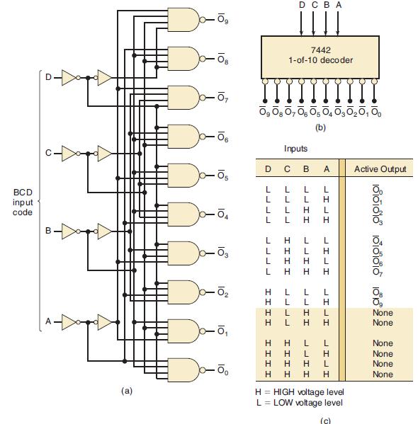
How does the 7445 differ from the 7442?
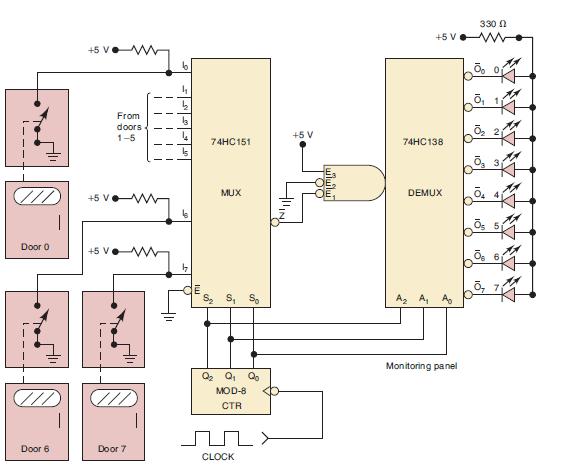
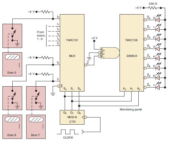
For the system of Figure 9-31, what will the security guard see on the monitoring panel when all of the doors are open?Figure 9-31 --1 Door 0 Door 6 +5 V +5 V From doors 1-5 Door 7 I T I H 411 9 4 13 4 mi E 74HC151 3 MUX So ရက် Q₂ Q₁ Qo MOD-8 CTR лу CLOCK +5 V +5 V 74HC138 DEMUX A₂
In the second technique, describe what is being divided.
What type of circuit provides the select inputs when a MUX is used asa parallel-to-serial converter?
Why are there no cascading inputs on a Quartus comparator megafunction?
What is a floating bus?
What will the output levels be when MR = HIGH and both OE inputsare held low?
What is the function of a bus driver?
Name two VHDL methods to describe a decoder’s operation.
In AHDL, how are tristate outputs implemented?
In the AHDL example, how are the logic states determined for the channelsthat are not selected?
What are the key operators used?
In VHDL, how is multiplication by 10 accomplished?
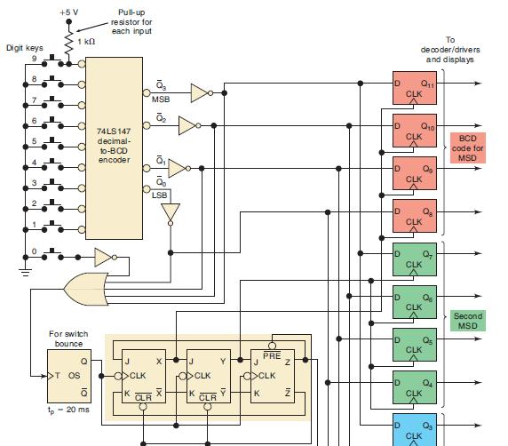
Describe the functions of each of the following parts of the keyboard entry circuit of Figure 9-16.(a) OR gate(b) 74147 encoder(c) One-shot(d) Flip-flops X, Y, Z(e) Flip-flops Q0 to Q11Figure 9-16 Digit keys +5 V 1 k0 For switch bounce 1p DT OS Q Ō 20 ms Pull-up resistor for each
Each segment of a typical 7-segment LED display is rated to operate at 10 mAat 2.7 V for normal brightness. Calculate the value of the current-limiting resistorneeded to produce approximately 10 mA per segment.
Show how to use 74LS138s to form a 1-of-16 decoder.
The 74154 is a 4-to-16 decoder with two active-LOW enable inputs. How many pins (including power and ground) does this IC have?
What are the reasons for having registers with common I/O lines?
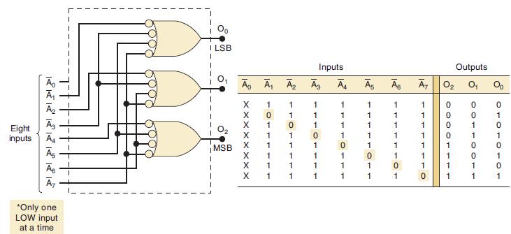
Determine the outputs of the encoder in Figure 9-13 when A̅3 and A̅5 are simultaneously LOW.Figure 9-13 KKKKKKKK Eight inputs A *Only one LOW input at a time 6988 food ILSB MSB Ã₁ X xxxxx X Ã₁ 101 1 1 1 A₂ A3 1 1 0 X 1
In VHDL, how are tristate outputs implemented?
In the VHDL example, how are the logic states determined for the channels that are not selected?
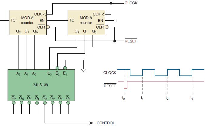
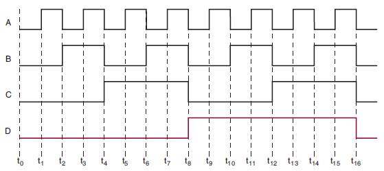
Figure 9-73 shows how a decoder can be used in the generation of control signals. Assume that a RESET pulse has occurred at time t0, and determine the CONTROL waveform for 32 clock pulses.Figure 9-73 TC MOD-8 counter CLK EN CLR Q₂ Q₁ Qo A₂ A₁ Ap 74LS138 E₂ E₂ E₁ TC 07 06 05 04 03 0₂
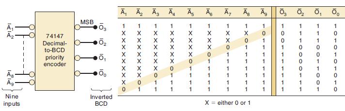
Determine the states of the outputs in Figure 9-14 when A̅5, A̅7, and A̅3 are LOW and all other inputs are HIGH.Figure 9-14 KAK 19. -19₁ Nine inputs 74147 Decimal- to-BCD priority encoder MSB 03 1 OI IO 10 A₁ A₂ 1 X X Inverted BCD X xxxo X 0 XX01 Ā3 Ã₁ 1 -XXXXXXOTT K X -xxxXX
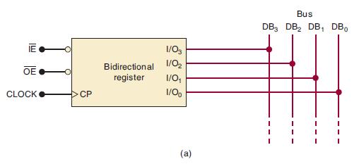
Redraw Figure 9-53(a) using the bundled line representation. Figure 9-53(a) ml OE CLOCK CP Bidirectional register 1/03 1/0₂2 1/0₁ 1/0⁰ (a) Bus DB DB₂ DB₁ DBo I I
What is the purpose of each control input and output on a 74148 encoder?
Modify the circuit of Figure 9-73 to generate a CONTROL waveform that goes LOW from t20 to t24.Figure 9-73 TC MOD-8 counter CLK EN CLR Q₂ Q₁ Qo A₂ A₁ Ap 74LS138 E₂ E₂ E₁ TC 07 06 05 04 03 0₂ 0₁ 00 MOD-8 counter CLK EN CLR Q₂ Q₁ Qo 1 CLOCK RESET CONTROL CLOCK RESET
A technician tests the circuit of Figure 9-4 by using a set of switches to apply the input code at A4 through A0. She runs through each possible input code and checks the corresponding decoder output to see if it is activated. She observes that all of the odd-numbered outputs respond correctly, but
(a) The 7442 decoder of Figure 9-5 does not have an ENABLE input. However, we can operate it as a 3-line-to-8-line decoder by not using outputs O̅8 and O̅9 and by using the D input as an ENABLE. This is illustrated in Figure 9-74. Describe how this arrangement works as an enabled 1-of-8 decoder,
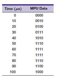
A technician wires the outputs from a BCD counter to the inputs of the decoder/driver of Figure 9-8. He applies pulses to the counter at a very slow rate and observes the LED display, which is shown below, as the counter counts up from 0000 to 1001. Examine this observed sequence carefully and try
Consider the waveforms in Figure 9-75. Apply these signals to the 74LS138 as follows:Assume that E̅1 and E̅2 are tied LOW, and draw the waveforms for outputs O̅0, O̅3, O̅6, and O̅7.Figure 9-75 A → Ao B→ A₁ C→ A₂ D→ E3
Modify the circuit of Figure 9-6 so that relay K1 stays energized from PGT 3 to 5 and K2 stays energized from PGT 6 to 9.Figure 9-6 1 pps CLOCK 24 V 03 Ō₂ OV 24 V OV 0 74ALS163 CLK ENT ENP DCBA CLR LOAD I I 1 I I RCO K₁ energized 8888 QD QB QA (a) I 1 I K₂ energized 1 2 3 4 5 6 7 8 9 10 11
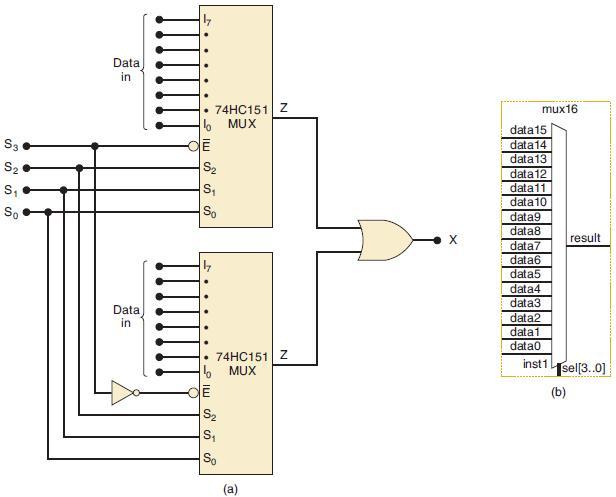
The circuit in Figure 9-22(a) uses two 74HC151s, an INVERTER, and an OR gate. Describe this circuit’s operation.Figure 9-22 S3 S₂ SSS So Data in Data in • 74HC151 Z lo MUX -OE S₂ S₁₂₁ So • 74HC151 Z b MUX -OE E S₂ S₁ So (a) X data15 data14 data13 mux16 data 12 data11 data
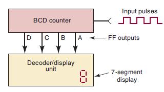
Show how to connect BCD-to-7-segment decoder/drivers and LED 7-segment displays to the counter circuit of Figure 7-22. Assume that each segment is to operate at approximately 10 mA at 2.5 V.Figure 7-22 D BCD counter C B A Decoder/display unit Input pulses n FF outputs - 7-segment display
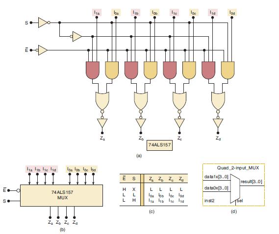
Determine the input conditions required for each Z output in Figure 9-23 to take on the logic level of its corresponding I0 input. Repeat for I1.Figure 9-23 mi E SO S IW E 12 116 116 11d los loo loo lod 74ALS157 MUX Za Zo Zo Zo (b) 110 H E S L L UUUUUUU (a) X JI х 8 100 L Zo Zo Zo Zo L L L L los
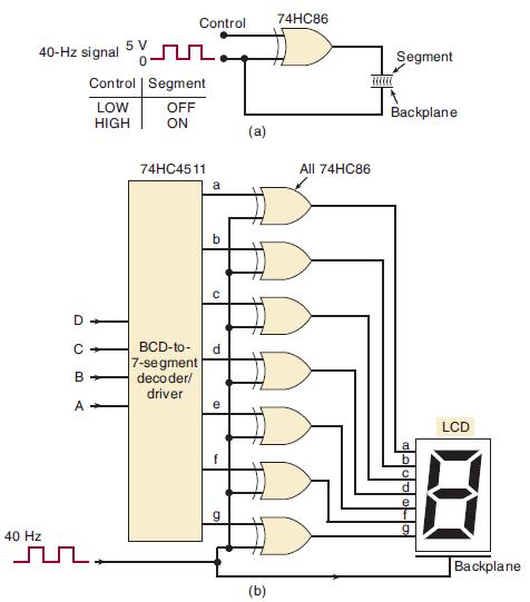
(a) Refer to Figure 9-10 and draw the segment and backplane waveforms relative to ground for CONTROL = 0. Then draw the waveform of segment voltage relative to backplane voltage.(b) Repeat part (a) for CONTROL = 1.Figure 9-10 40-Hz signal 40
Examine Figure 9-31 carefully and describe the complete operation.Figure 9-31 Door 0 Door 6 +5 V +5 V +5 V ---1 From doors 1-5 Door 7 I II 1 B N h E 74HC151 MUX S₂ S₁ S₂ Q₂ Q₁ Qo MOD-8 CTR CLOCK +5 V ليالي الي +5 VW 74HC138 330 Ω Ō₂ 0₂ DEMUX 04 A₂ A₁ A₂ 6⁰⁰
The BCD-to-7-segment decoder/driver of Figure 9-8 contains the logic for activating each segment for the appropriate BCD inputs. Design the logic for activating the g segment.Figure 9-8 D C BCD input B A Blanking controls LED test input BCD- to- 7-segment decoder/ driver BI/RBO RBI LT a 7446 or
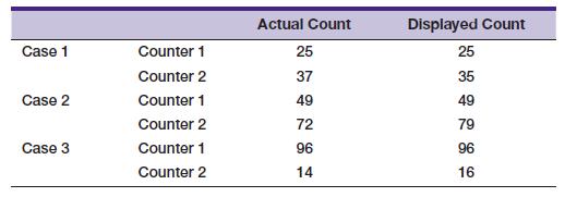
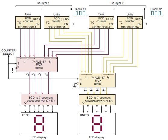
Consider the circuit of Figure 9-24. A test performed on this circuit yields the result shown in Table 9-3. What is the probable circuit fault?Table 9-3Figure 9-24 Case 1 Case 2 Case 3 Counter 1 Counter 2 Counter 1 Counter 2 Counter 1 Counter 2 Actual Count 25 37 49 72 96 14 Displayed
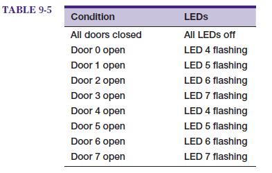
The security monitoring system of Figure 9-31 is tested and the results are recorded in Table 9-5. What are the possible faults that could produce these results?Figure 9-31 TABLE 9-5 Condition All doors closed Door 0 open Door 1 open Door 2 open Door 3 open Door 4 open Door 5 open Door 6 open Door
Showing 400 - 500
of 1612
1
2
3
4
5
6
7
8
9
10
11
12
13
14
15
Last
Step by Step Answers
![(IN[n OUT[n] OUT[4] (IN[1] OUT[5] = (IN[2] = - - 3] + IN[n 2] + IN[n + IN[2] + IN[3] + IN[3] + IN[4] 1] +](https://dsd5zvtm8ll6.cloudfront.net/images/question_images/1700/2/0/3/77165570cfb7aedb1700203772653.jpg)
![Sample n IN[n] (V) OUT[n] (V) 1 0 0 2 0 0 3 0 0 4 0 5 10 6 10 7 10 8 10 9 10 10 10](https://dsd5zvtm8ll6.cloudfront.net/images/question_images/1700/2/0/3/61665570c60400201700203617527.jpg)