New Semester
Started
Get
50% OFF
Study Help!
--h --m --s
Claim Now
Question Answers
Textbooks
Find textbooks, questions and answers
Oops, something went wrong!
Change your search query and then try again
S
Books
FREE
Study Help
Expert Questions
Accounting
General Management
Mathematics
Finance
Organizational Behaviour
Law
Physics
Operating System
Management Leadership
Sociology
Programming
Marketing
Database
Computer Network
Economics
Textbooks Solutions
Accounting
Managerial Accounting
Management Leadership
Cost Accounting
Statistics
Business Law
Corporate Finance
Finance
Economics
Auditing
Tutors
Online Tutors
Find a Tutor
Hire a Tutor
Become a Tutor
AI Tutor
AI Study Planner
NEW
Sell Books
Search
Search
Sign In
Register
study help
computer science
digital systems principles and application
Digital Systems Principles And Application 12th Edition Ronald Tocci, Neal Widmer, Gregory Moss - Solutions
A photodetector circuit is being used to generate a pulse each time a customer walks into a certain establishment. The pulses are fed to an eight-bit counter. The counter is used to count these pulses as a means for determining how many customers have entered the store. After closing the store, the
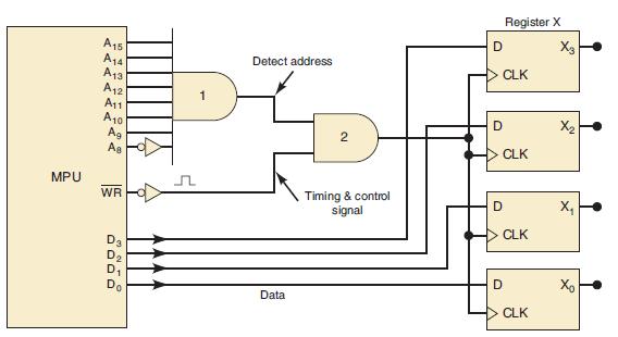
Suppose that the circuit of Figure 5-58 is malfunctioning so that data are being transferred to X for either of the address codes 11111110 or 11111111. What are some circuit faults that could be causing this?Figure 5-58 MPU A15 A14 A13 A12 A11 A 10 Ag As WR D3 Л Detect address Data 2 Timing &
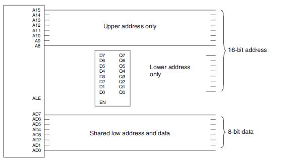
Many microcontrollers share the same pins to output the lower address and transfer data. In order to hold the address constant while the data are transferred, the address information is stored in a latch which is enabled by the control signal ALE (address latch enable) as shown in Figure 5-97.
Modify the circuit of Figure 5-58 so that the MPU has eight data output lines connected to transfer eight bits of data to an eight-bit register made up of two 74HC175 ICs. Show all circuit connections.Figure 5-58 MPU A15 A14 A13 A12 A11 A 10 Ag As WR D3 Л Detect address Data 2 Timing &
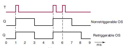
Refer to the waveforms in Figure 5-61(a). Change the OS pulse duration to 0.5 ms and determine the Q output for both types of OS. Then repeat using a OS pulse duration of 1.5 ms.Figure 5-61(a) T 012 3 4 Л Nonretriggerable OS 1 T 5 6 7 8 9 Retriggerable OS ms
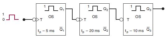
Figure 5-98 shows three nonretriggerable one-shots connected in a timing chain that produces three sequential output pulses. Note the “1” in front of the pulse on each OS symbol to indicate nonretriggerable operation. Draw a timing diagram showing the relationship between the input pulse and
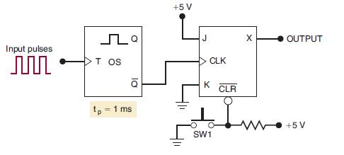
A retriggerable OS can be used as a pulse-frequency detector that detects when the frequency of a pulse input is below a predetermined value. A simple example of this application is shown in Figure 5-99. The operation begins by momentarily closing switch SW1.(a) Describe how the circuit responds to
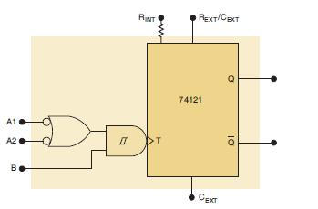
Refer to the logic symbol for a 74121 nonretriggerable one-shot in Figure 5-62.(a) What input conditions are necessary for the OS to be triggered by a signal at the B input?(b) What input conditions are necessary for the OS to be triggered by a signal at the A1 input?Figure 5-62 A1 A2 B д Д
The output pulse width from a 74121 OS is given by the approximate formula tp ≈ 0.7RTCT where RT is the resistance connected between the REXT/CEXT pin and VCC, and CT is the capacitance connected between the CEXT pin and the REXT/CEXT pin. The value for RT can be varied between 2 and 40 kΩ, and
Show how to use a 74LS14 Schmitt-trigger INVERTER to produce an approximate square wave with a frequency of 10 kHz.
Design a 555 free-running oscillator to produce an approximate square wave at 40 kHz. C should be kept at 500 pF or greater.
Refer to the counter circuit in Figure 5-48. Assume that all asynchronous inputs are connected to VCC. When tested, the circuit waveforms appear as shown in Figure 5-101. Consider the following list of possible faults. For each one, indicate “yes” or “no” as to whether it could cause the
A 555 oscillator can be combined with a J-K flip-flop to produce a perfect (50 percent duty cycle) square wave. Modify the circuit of Problem 5-46 to include a J-K flip-flop. The final output is still to be a 40-kHz square wave.Data from Problem 5-46Design a 555 free-running oscillator to produce
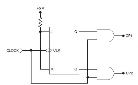
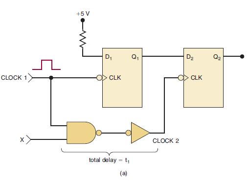
The circuit in Figure 5-100 can be used to generate two nonoverlapping clock signals at the same frequency. These clock signals were used in early microprocessor systems that required four different clock transitions to synchronize their operations.(a) Draw the CP1 and CP2 timing waveforms if CLOCK
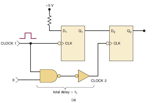
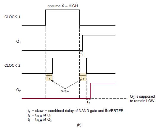
Consider the situation of Figure 5-67 for each of the following sets of timing values. For each, indicate whether or not flip-flop Q2 will respond correctly.Figure 5-67 (a)* Each FF: TPLH = 12 ns; tpHL = 8 ns; ts = 5 ns; th 8 ns; tpHL 6ns 5ns (b) NAND gate: tpLH (c) INVERTER: tpLH = 7ns; tpHL = (d)
Design a 555 timer circuit that will produce a 10 percent duty-cycle 5-kHz waveform. Choose a capacitor greater than 500 pF and resistors less than 100 kΩ. Draw the circuit diagram with pin numbers labeled.
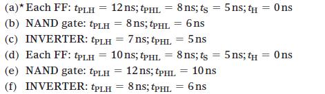
Show and explain how the clock skew problem in Figure 5-67 can be eliminated by the appropriate insertion of two INVERTERs.Figure 5-67 CLOCK 1 +5 V D₁ O CLK total delay = 1₁ (a) CLOCK 2 D₂ CLK Q₂
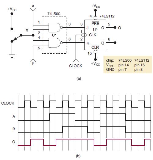
Refer to the circuit of Figure 5-102. Assume that the ICs are of the TTL logic family. The Q waveform was obtained when the circuit was tested with the input signals shown and with the switch in the “up” position; it is not correct. Consider the following list of faults, and for each indicate
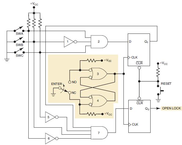
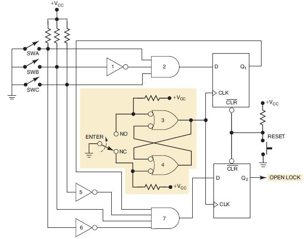
The circuit of Figure 5-103 functions as a sequential combination lock. To operate the lock, proceed as follows:1. Momentarily activate the RESET switch.2. Set the switches SWA, SWB, and SWC to the first part of the combination. Then momentarily toggle the ENTER switch back and forth.3. Set the
When the combination lock of Figure 5-103 is tested, it is found that entering the correct combination does not open the lock. A logic probe check shows that entering the correct first combination sets Q1 HIGH, but entering the correct second combination produces only a momentary pulse at Q2.
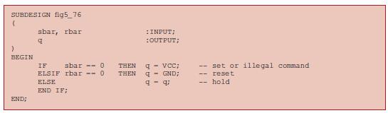
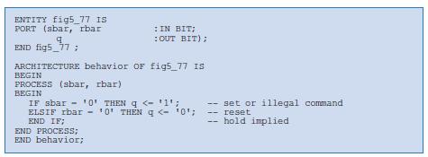
Simulate the HDL design for a NAND latch given in Figure 5-76 (AHDL) or Figure 5-77 (VHDL). What does this S-R latch do if an “invalid” input command is applied? Since we know that any S-R latch can have an unusual output result when an invalid input command is applied, you should simulate that
For each statement indicate what type of FF is being described.(a) Has a SET and a CLEAR input but does not have a CLK input(b) Will toggle on each CLK pulse when its control inputs are both HIGH(c) Has an ENABLE input instead of a CLK input(d) Is used to transfer data easily from one FF register
Define the following terms.(a) Asynchronous inputs(b) Edge-triggered(c) Shift register(d) Frequency division(e) Asynchronous (jam) transfer(f) State transition diagram(g) Parallel data transfer(h) Serial data transfer(i) Retriggerable one-shot(j) Schmitt-trigger inputs
Modify the latch description given in Figure 5-76 (AHDL) or Figure 5-77 (VHDL) to make the S-R reset if an invalid input is applied. Simulate the design.Figure 5-76Figure 5-77 SUBDESIGN fig5_76 sbar, rbar 9 ( ) BEGIN END; IF sbar 0 ELSIF rbar -- 0 ELSE END IF; :INPUT; :OUTPUT; THEN q vcc; THEN q-
Write an HDL design file for an active-HIGH input S-R latch. Functionally simulate the design.
Add inverted outputs to the HDL NAND latch designs given in Figure 5-76 or Figure 5-77. Verify correct operation by simulation.Figure 5-76Figure 5-77 SUBDESIGN fig5_76 sbar, rbar 9 ( ) BEGIN END; IF sbar 0 ELSIF rbar -- 0 ELSE END IF; :INPUT; :OUTPUT; THEN q vcc; THEN q- GND; q-q; set or illegal
Simulate the AHDL or VHDL design for a D latch.
Create a four-bit transparent latch with one enable input and simulate (functional) your design.(a) Use the primitive DLATCH in a schematic design file.(b) Use the LPM_LATCH in a schematic design file.(c) Use an HDL design file. Modify the D latch design given, by using arrays for the data inputs
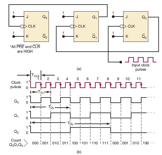
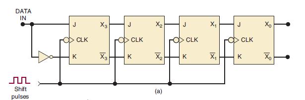
(a) Create the four-bit shift register in Figure 5-46(a) using the LPM_ FF megafunction in a schematic and functionally simulate.(b) Create the four-bit shift register in Figure 5-46(a) using an HDL and functionally simulate.Figure 5-46(a) DATA J X₂ J CLK VII X3 K X₂
A toggle (T) flip-flop has a single control input (T). When T = 0, the flipflop is in the no change state, similar to a JKFF with J = K = 0. When T = 1, the flip-flop is in the toggle mode, similar to a JKFF with J = K = 1. Create an HDL design for a T flip-flop and functionally simulate.
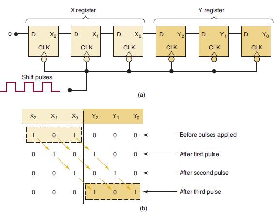
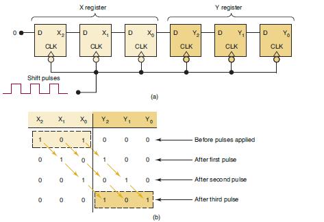
Create the two register circuit shown in Figure 5-47. Include a serial data_in on the X register and functionally simulate.(a) Use two LPM_SHIFTREG megafunctions in a schematic.(b) Use an HDL.Figure 5-47 0 D X₂ Shift pulses nnn 0 X₂ 0 CLK X₁ 0 1 0 X
(a) Write an AHDL design file for the FF circuit shown in Figure 5-67.(b) Write a VHDL design file for the FF circuit shown in Figure 5-67.Figure 5-67 CLOCK 1 +5 V D₁ CLK total delay 1₁ (a) CLOCK 2 D₂ CLK
Simulate (timing) the operation of the circuit in Problem 5-67. The simulation results should match the results in Figure 5-67.Data from Problem 5-67Write an AHDL design file for the FF circuit shown in Figure 5-67.Write a VHDL design file for the FF circuit shown in Figure 5-67.Figure 5-67 CLOCK
(a) Write an AHDL design file to implement the entire circuit of Figure 5-103.(b) Write a VHDL design file to implement the entire circuit of Figure 5-103.Figure 5-103. SWA SWB SWC +Vcc Live WW www 6 ENTER Ó NO ONC 2 +Voc +Vcc D CLK D CLR CLR CLK ģ Q₂ +Vcc RESET OPEN LOCK
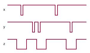
Assuming that Q = 0 initially, apply the x and y waveforms of Figure 5-87 to the SET and RESET inputs of a NAND latch, and determine the Q and Q̅ waveforms.Figure 5-87 X Z ㅠ ㅜ
What is the MOD number of the counter in question 2?
Name three common applications of flip-flops that were used in the quadrature encoder system.
Which FF timing parameters indicate the time it takes the Q output to respond to an input?
What is the distinguishing hardware characteristic of latching logic circuits?
True or false: Synchronous circuits always violate set and hold times becausethe outputs change on the active clock edge.
When should synchronization circuits be used?
How does a DFF identify which input changes first?
What is the purpose of the XOR gate in the event detector circuit?
True or false: Asynchronous data transfer uses the CLK input.
What does the designer need to know in order to use a logic primitive?
What will be the states of Q and Q̅ after a FF has been reset (cleared)?
What is the major advantage of serial transfer over parallel transfer?
In AHDL, where are multiple instances of a component declared?
When a latch is set, what are the states of Q and Q̅?
Why was a single DFF serving as the sequence detector inadequate tokeep track of absolute position?
How many FFs are required for a counter that will count 0 to 25510?
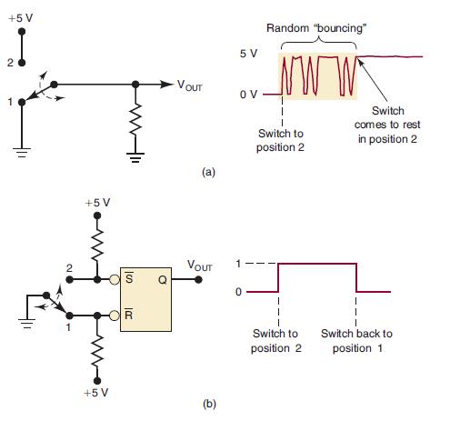
It is almost impossible to obtain a “clean” voltage transition from a mechanical switch because of the phenomenon of contact bounce. This is illustrated in Figure 5-9(a), where the action of moving the switch from contact position 1 to 2 produces several output voltage transitions as the switch
What is meant by the term edge-triggered?
Where is pulse width measured?
How does a Schmitt-trigger logic device operate differently from a standard logic device?
True or false: When a nonretriggerable OS is pulsed while it is in its quasi-stable state, the output is not affected.
Explain why the S and R inputs affect Q only during the active transition of CLK.
Determine the approximate frequency and duty cycle of the 555 oscillator for RA = RB = 2.2 kΩ and C = 2000 pF.
Does a J-K flip-flop have any ambiguous input conditions?
True or false: The Q output will equal the level at the D input at all times.
True or false: A D latch is in its transparent mode when EN = 0.
Can a D flip-flop respond to its D and CLK inputs while P̅R̅E̅ = 1?
True or false: A FF that has an fMAX rating of 25 MHz can be reliably triggered by any CLK pulse waveform with a frequency below 25 MHz.
True or false: The propagation delay time must exceed the hold time requirements in order for synchronous flip-flop circuit to work reliably.
What is the major characteristic of sequential circuits?
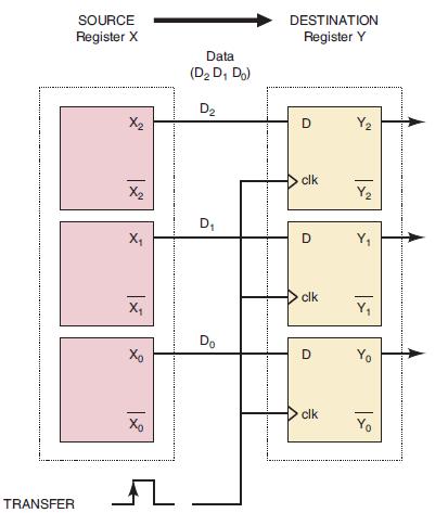
If J-K flip-flops were used in the registers of Figure 5-45, how many total interconnections would be required from register X to register Y?Figure 5-45 TRANSFER SOURCE Register X X₂ X₁ X₁ Xo Xo A Data (D₂ D₁ Do) D₂ D₁ Do DESTINATION Register
How are DFFs used to synchronize signals?
Assume CLK is 1 MHz, 50% duty cycle. If the input signal changes state on the falling edge of CLK, what will the output EDGE signal look like?
Which type of FF is best suited for synchronous transfer because it requires the fewest interconnections from one FF to the other?
Refer to Figure 5-47. Assume that the initial contents of the registers are X2 = 0, X1 = 1, X0 = 0, Y2 = 1, Y1 = 1, Y0 = 0. Also assume that the D input of FFX2 is held HIGH. Determine the value of each FF output after the occurrence of the fourth shift pulse.Figure 5-47 D X₂ Shift
In the Altera system, where can you find information on primitives and library functions?
True or false: The S̅E̅T̅ input can never be used to make Q = 0.
How do you distinguish between multiple instances of a component?
What timing issues are at fault in Figure 5-52?Figure 5-52 A B CLOCK Absolute shaft encoder A edge Q[n-1] 194 Q[n-1] B edge Direction decoder UP/DN counter Enable Direction UP/DN CLK Position.
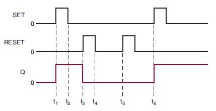
Assume that Q = 0 initially, and determine the Q waveform for the NOR latch inputs of Figure 5-11.Figure 5-11 SET RESET Q 0 0 0 1 1 1 13 14 15 16
What is the only way to cause the Q output of a NOR latch to change from 1 to 0?
Where is rise time measured?
True or false: The CLK input will affect the FF output only when the active transition of the control input occurs.
What determines the tp value for a OS?
Can J-K FFs be used for parallel data transfer?
What J-K input condition will always set Q upon the occurrence of the active CLK transition?
What is the advantage of crystal-controlled clock generator circuits over RC-controlled circuits?
True or false: In a D latch, the D input can affect Q only when EN = 1.
The minimum amount of time that a control input must be stable before the clock edge is called _______________.
List the conditions necessary for a positive-edge-triggered J-K flip-flop with active-LOW asynchronous inputs to toggle to its opposite state.
True or false: Synchronous data transfer requires less circuitry than asynchronous transfer.
To analyze a synchronous circuit, where can the control inputs be found that will determine the output changes?
What is the key VHDL element that allows the explicit description of clocked logic circuits?
In which form of data transfer does the source of the data not lose its data?
When power is first applied to any FF circuit, it is impossible to predict the initial states of Q and Q̅. What can be done to ensure that a NAND latch always starts off in the Q = 1 state?
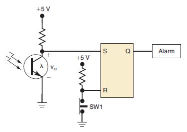
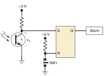
If the NOR latch in Figure 5-12 were replaced by a NAND latch, why wouldn’t the circuit work properly?Figure 5-12 +5 V Vo +5 V SW1 S R Q Alarm
Figure 5-12 shows a simple circuit that can be used to detect the interruption of a light beam. The light is focused on a phototransistor that is connected in the common-emitter configuration to operate as a switch. Assume that the latch has previously been cleared to the 0 state by momentarily
In AHDL, what operator is used to “connect” signals?
What is the frequency of the output of the eighth FF when the input clock frequency is 512 kHz?
Where is fall time measured?
Define the setup time and hold time requirements of a clocked FF.
Describe how a retriggerable OS operates differently from a nonretriggerable OS.
The minimum amount of time a control input must remain stable after a clock edge is called _______________.
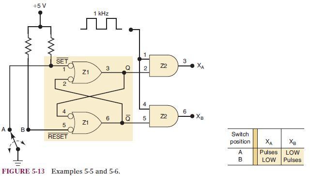
Analyze and describe the operation of the circuit in Figure 5-13.Figure 5-13 A B +5 V SET 2 5 RESET 1 kHz nn Z1 Z1 3 6 FIGURE 5-13 Examples 5-5 and 5-6. O la 2 5 Z2 72 3 6 XA Switch position A B XA XB LOW Pulses Pulses LOW
Which library defines the std_logic data types?
Showing 1000 - 1100
of 1612
First
3
4
5
6
7
8
9
10
11
12
13
14
15
16
17
Step by Step Answers
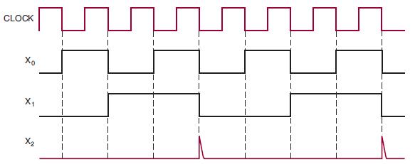
![A B CLOCK Absolute shaft encoder A edge Q[n-1] 194 Q[n-1] B edge Direction decoder UP/DN counter Enable](https://dsd5zvtm8ll6.cloudfront.net/images/question_images/1699/7/0/2/736654f67d00cd901699702736828.jpg)