New Semester
Started
Get
50% OFF
Study Help!
--h --m --s
Claim Now
Question Answers
Textbooks
Find textbooks, questions and answers
Oops, something went wrong!
Change your search query and then try again
S
Books
FREE
Study Help
Expert Questions
Accounting
General Management
Mathematics
Finance
Organizational Behaviour
Law
Physics
Operating System
Management Leadership
Sociology
Programming
Marketing
Database
Computer Network
Economics
Textbooks Solutions
Accounting
Managerial Accounting
Management Leadership
Cost Accounting
Statistics
Business Law
Corporate Finance
Finance
Economics
Auditing
Tutors
Online Tutors
Find a Tutor
Hire a Tutor
Become a Tutor
AI Tutor
AI Study Planner
NEW
Sell Books
Search
Search
Sign In
Register
study help
computer science
digital systems principles and application
Digital Systems Principles And Application 12th Edition Ronald Tocci, Neal Widmer, Gregory Moss - Solutions
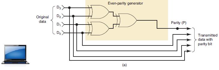
Determine the parity generator’s output for each of the following sets of input data, D3D2D1D0: (a) 0111; (b) 1001; (c) 0000; (d) 0100. Refer to Figure4-25(a).Figure 4-25(a) Original data D₂ D₁ Do Even-parity generator (a) Parity (P) Transmitted data with parity bit
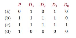
Determine the parity checker’s output [see Figure 4-25(b)] for each of the following sets of data from the transmitter:Figure 4-25(b) (a) (b) (c) (d) D3 D2 1 1 D₁ 0 1 1 1 0 P 0 1 1 1 1 1 1 10 0 0 Do 0 0 1 0
Design a logic circuit that will allow a signal to pass to the output only when control inputs B and C are both HIGH; otherwise, the output will stay LOW.
Design a logic circuit that allows a signal to pass to the output only when one, but not both, of the control inputs are HIGH; otherwise, the output will stay HIGH.
Refer to the circuit of Figure 4-36. A technician uses a logic probe to determine the conditions at the various IC pins. The results are recorded in the figure. Examine these results and determine if the circuit is working properly. If not, suggest some of the possible faults.Figure 4-36
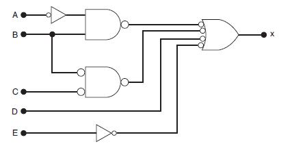
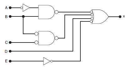
Design a logic circuit with input signal A, control input B, and outputs X and Y to operate as follows:1. When B = 1, output X will follow input A, and output Y will be 0.2. When B = 0, output X will be 0, and output Y will follow input A.
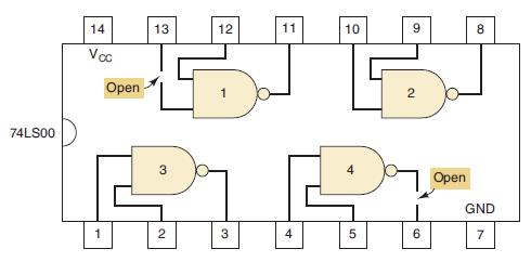
What would a logic probe indicate at pin 13 and at pin 6 of Figure 4-37?Figure 4-37 74LS00 14 Voc 1 Open 13 3 2 12 3 11 10 5 9 2 6 Open GND 7
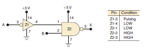
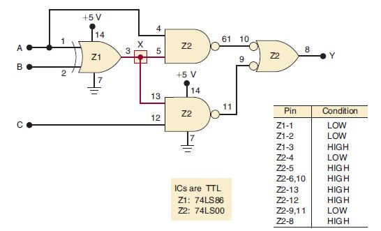
Refer to the circuit of Figure 4-38 and the recorded logic probe indications. What are some of the possible faults that could produce the recorded results? Assume that the ICs are TTL.Figure 4-38 A B ве 3 Z1 4 1 2 Note: Vcc and ground connections to each IC are not shown Z2 X Condition Pin Z1-3
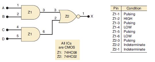
Consider the CMOS circuit of Figure 4-40 and the accompanying logic probe indications. What is the most probable circuit fault?Figure 4-40 A B C D 2 4 10 5 Z1 Z1 3 6 3 2 N Z2 All ICs are CMOS Z1: 74HC08 Z2: 74HC02 Condition Pin Z1-1 Pulsing Z1-2 HIGH Z1-3 Pulsing Z1-4 LOW Z1-5 Pulsing Z1-6 LOW Z2-3
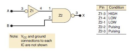
Consider the circuit of Figure 4-41. Output Y is supposed to go HIGH for either of the following conditions:1. A = 1, B = 0 regardless of the level on C2. A = 0, B = 1, C = 1You may wish to verify these results for yourself.When the circuit is tested, the technician observes that output Y goes HIGH
Assume there is an eight-bit array named P1, as shown in Figure 4-52, and another four-bit array is named P5.(a) Write the bit designation for the most significant bit of P1.(b) Write the bit designation for the least significant bit of P5.(c) Write an expression that causes the least significant
Express the following bit pattern’s numeric value in binary, hex, and decimal using AHDL and VHDL notation: 11001
Declare a four-bit input named keypad using AHDL.
Declare a four-bit input named keypad using VHDL.
Declare three signals in VHDL that are single bits named too_hot, too_cold, and just_right. Combine (concatenate) these three bits into a three-bit signal called temp_status, with hot on the left and cold on the right.
A coin detector in a vending machine accepts quarters, dimes, and nickels and activates the corresponding digital signal (Q, D, N) only when the correct coin is present. It is physically impossible for multiple coins to be present at the same time. A digital circuit must use the Q, D, and N signals
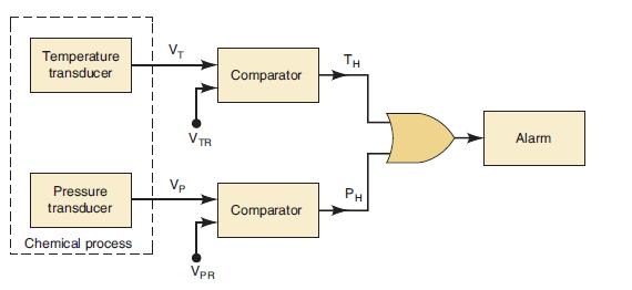
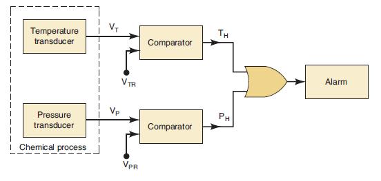
In many industrial control systems, it is required to activate an output function whenever any one of several inputs is activated. For example, in a chemical process it may be desired that an alarm be activated whenever the process temperature exceeds a maximum value or whenever the pressure goes
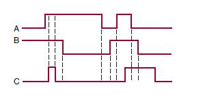
(a) Draw the output waveform for the OR gate of Figure 3-52.(b) Suppose that the A input in Figure 3-52 is unintentionally shorted to ground (i.e., A = 0). Draw the resulting output waveform.(c) Suppose that the A input in Figure 3-52 is unintentionally shorted to the +5 V supply line (i.e., A =
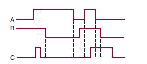
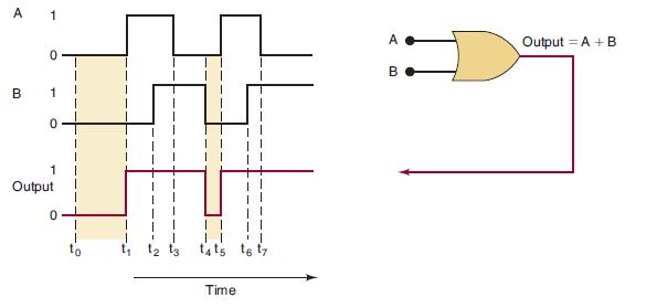
Determine the OR gate output in Figure 3-5. The OR gate inputs A and B are varying according to the timing diagrams shown. For example, A starts out LOW at time t0, goes HIGH at t1, back to LOW at t3, and so on.Figure 3-5 A B 1 Output 0 Time A B Output = A + B
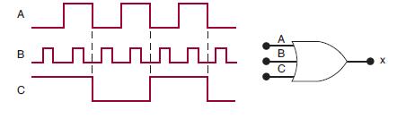
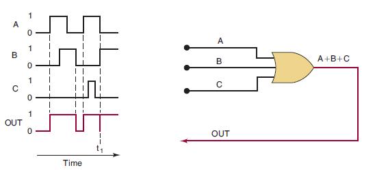
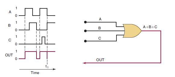
a. For the situation depicted in Figure 3-6, determine the waveform at the OR gate output.Figure 3-6b. What would happen to the glitch in the output in Figure 3-6 if input C sat in the HIGH state while A and B were changing at time t1?Figure 3-6 A B C OUT 0 1 0 0 1 0 Time T 1 A B O OUT A+B+C
A three-input OR gate should be producing a logic 0 at its output but instead it is producing a logic 1. How can you determine which of the three inputs is incorrect?
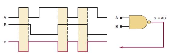
Determine the output x from the AND gate in Figure 3-9 for the given input waveforms. B 1 0 1 1 0 to 1₁ 1₂ 13 14 t5 16 17 A B x = AB
Read the statements below concerning an OR gate. At first, they may appear to be valid, but after some thought you should realize that neither one is always true. Prove this by showing a specific example to refute each statement.(a) If the output waveform from an OR gate is the same as the waveform
How many different sets of input conditions will produce a HIGH output from a five-input OR gate?
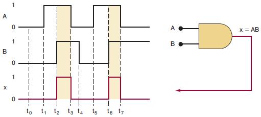
a. Determine the output waveform for the AND gate shown in Figure 3-10.b. What will happen to the x output waveform in Figure 3-10 if the B input is kept at the 0 level?Figure 3-10 A MMMMM B X _L A B X
A three-input AND gate should be producing a logic 1 at its output but instead it is producing a logic 0. How can you determine which of the three inputs is incorrect?
Change the OR gate in Figure 3-52 to an AND gate.(a) Draw the output waveform.(b) Draw the output waveform if the A input is permanently shorted to ground.(c) Draw the output waveform if A is permanently shorted to +5 V.Figure 3-52 A B C | பப்பப்பம் A B C X
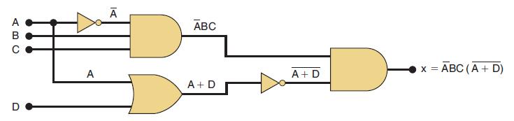
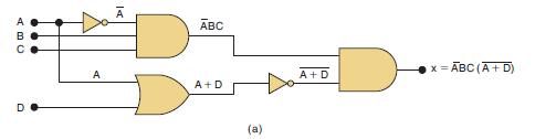
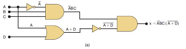
Analyze the operation of Figure 3-15(a) by creating a table showing the logic state at each node of the circuit.Figure 3-15(a) ABC O A ABC A+ D (a) A+ D = ABC (A + D) X =
Refer to Figure 3-4. Modify the circuit so that the alarm is to be activated only when the pressure and the temperature exceed their maximum limits at the same time.Figure 3-4 Temperature transducer Pressure transducer 1 Chemical process VTR VPR Comparator Comparator TH PH Alarm
Change the OR gate in Figure 3-6 to an AND gate and draw the output waveform.Figure 3-6 B C OUT 1 Time A B C OUT A+B+C
Draw the circuit diagram to implement the expression x = (A + B) (B̅ + C).
Determine the waveform at the output of a NOR gate for the input waveforms shown in Figure 3-20.Figure 3-20 A B X 0 1 0 1 0 A B x = A + B
Suppose that you have an unknown two-input gate that is either an OR gate or an AND gate. What combination of input levels should you apply to the gate’s inputs to determine which type of gate it is?
Determine the Boolean expression for a three-input NOR gate followed by an INVERTER.
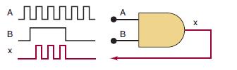
Determine the output waveform of a NAND gate having the input waveforms shown in Figure 3-23.Figure 3-23 A B x | I A B x = AB
True or false: No matter how many inputs it has, an AND gate will produce a HIGH output for only one combination of input levels.
Apply the A waveform from Figure 3-23 to the input of an INVERTER. Draw the output waveform. Repeat for waveform B.Figure 3-23 A B 닥 A B x = AB
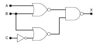
Implement the logic circuit that has the expression using only NOR and NAND gates. x= AB (C + D)
(a) Write the Boolean expression for output x in Figure 3-53(a). Determine the value of x for all possible input conditions, and list the values in a truth table.(b) Repeat for the circuit in Figure 3-53(b).Figure 3-53 A B A B O D (a) (b) X
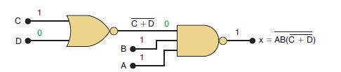
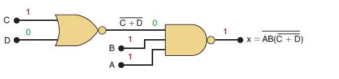
Determine the output level in Figure 3-24 for A = B = C = 1 and D = 0.Figure 3-24 D 0 A C+D 1 0 x = AB(C + D)
Create a complete analysis table for the circuit of Figure 3-15(b) by finding the logic levels present at each gate output for each of the 32 possible input combinations.Figure 3-15b A B O D E A+B (A + B)C (b) (A + B)C D + (A + B)C x = [D+ (A + B)C] E
(a) Change each OR to an AND, and each AND to an OR, in Figure 3-15(b). Then write the expression for the output.(b) Complete an analysis table.Figure 3-15b A B O D E A+B (A + B)C (b) (A + B)C D + (A + B)C x = [D+ (A + B)C] E
Simplify z = (A̅ + B) (A + B).
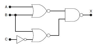
For each of the following expressions, construct the corresponding logic circuit, using AND and OR gates and INVERTERs.
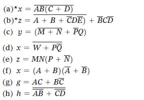
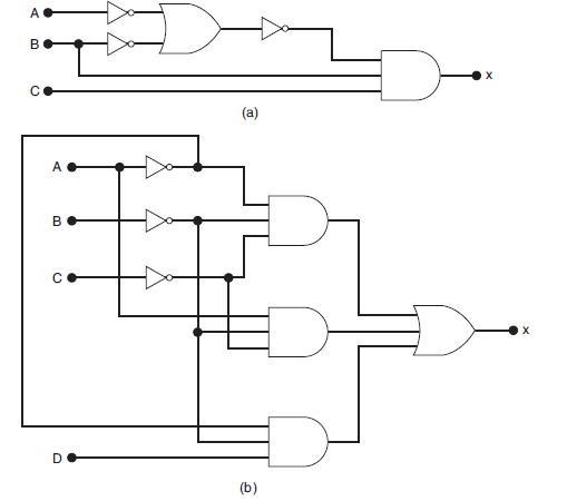
For each of the following expressions, construct the corresponding logic circuit, using AND and OR gates and INVERTERs. (a)*x = AB(C + D) (b)*2 = A + B + CDE) + BCD (c) y = (M + N + PQ) (d) x = W + PQ (e) z = MN(P + N) (f) x = (A + B) (A + B) (g) g = AC + BC (h) h = AB + CD
Simplify x = ACD + A̅BCD.
Simplify the expression to one having only single variables inverted. 2= (A + C). (B + D)
(a) Apply the input waveforms of Figure 3-54 to a NOR gate, and draw the output waveform.(b) Repeat with C held permanently LOW.(c) Repeat with C held HIGH.Figure 3-54 A B C . | | | | | -
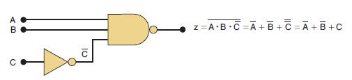
Determine the output expression for the circuit of Figure 3-28 and simplify it using DeMorgan’s theorems.Figure 3-28 B O 10 z = A·B ·C=A+B+C =Ā+B+C
In a certain manufacturing process, a conveyor belt will shut down whenever specific conditions occur. These conditions are monitored and reflected by the states of four logic signals as follows: signal A will be HIGH whenever the conveyor belt speed is too fast; signal B will be HIGH whenever the
Write the expression for the output of Figure 3-55, and use it to determine the complete truth table. Then apply the waveforms of Figure 3-54 to the circuit inputs, and draw the resulting output waveform.Figure 3-55Figure 3-54 A B I C X
Determine the truth table for the circuit of Figure 3-24.Figure 3-24 () D 0 B A C +D 1 x = AB(C + D)
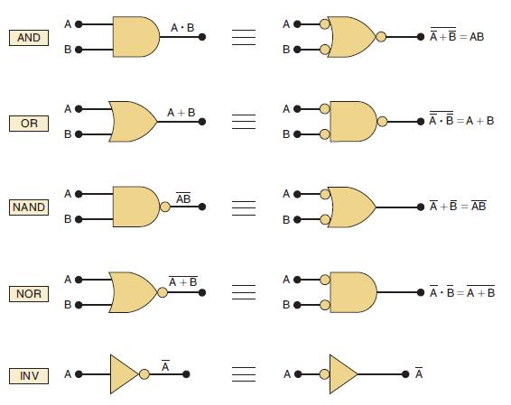
Give the interpretation of the two OR gate symbols.
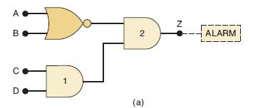
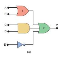
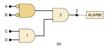
The logic circuit in Figure 3-37(a) is being used to activate an alarm when its output Z goes HIGH. Modify the circuit diagram so that it represents the circuit operation more effectively.Figure 3-37(a) A B C D 1 2 (a) N ALARM
Modify the circuits that were constructed in Problem 3-16 so that NAND gates and NOR gates are used wherever appropriate.Data from problem 3-16For each of the following expressions, construct the corresponding logic circuit, using AND and OR gates and INVERTERs. (a)*x = AB(C + D) (b)*2 = A + B +
When the output of the logic circuit in Figure 3-38(a) goes LOW, it activates another logic circuit. Modify the circuit diagram to represent the circuit operation more effectively. Figure 3-38(a) A B ce De E (a) N
Prove theorems (15a) and (15b) by trying all possible cases.Theorem 15 (15a) x + xy = x + y á + x = x + x (qSI)
(a) Simplify the following expression using theorems (13b), (3), and (4):(b) Simplify the following expression using theorems (13a), (8), and (6):Theorem 13Theorem 3Theorem 4Theorem 6Theorem 8 x = (M + N) (M + P) (N + P)
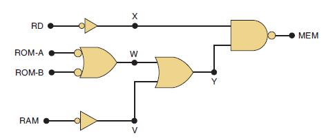
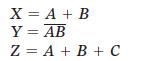
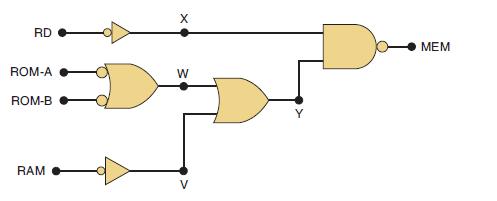
The logic circuit in Figure 3-39 generates an output, MEM, that is used to activate the memory ICs in a particular microcomputer. Determine the input conditions necessary to activate MEM.Figure 3-39 RD ROM-A ROM-B RAM W V MEM
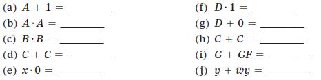
Complete each expression. (a) A + 1 = (b) A.A = (c) B-B = (d) C + C = (e) x 0 = (f) D.1 = (g) D + 0 = (h) C + C = (i) G + GF (j) y + wy =
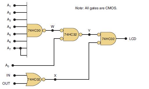
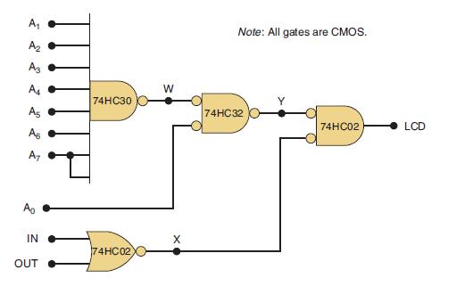
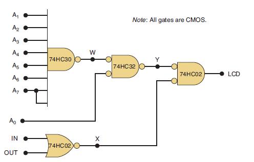
The logic circuit in Figure 3-40 is used to enable the liquid crystal display (LCD) of a handheld electronic device when the microcontroller is sending data to or receiving data from the LCD controller. The circuit will enable the display when LCD = 1. Determine the input conditions necessary to
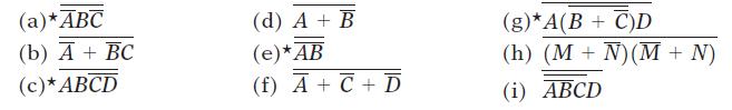
Simplify each of the following expressions using DeMorgan’s theorems. (a) * ABC (b) A + BC (c)* ABCD (d) A + B (e) * AB (f) A + C + D (g)*A(B+C)D (h) (M + N) (M + N) (i) ABCD
Compare the operation of a computer and a logic circuit in performing the simple logical operation of y = AB.
Use DeMorgan’s theorems to simplify the expression for the output of Figure 3-55.Figure 3-55 A® B 도 C X
Convert the circuit of Figure 3-53(b) to one using only NAND gates. Then write the output expression for the new circuit, simplify it using DeMorgan’s theorems, and compare it with the expression for the original circuit.Figure 3-53b A B C D (b) X
Convert the circuit of Figure 3-53(a) to one using only NOR gates. Then write the expression for the new circuit, simplify it using DeMorgan’s theorems, and compare it with the expression for the original circuit.Figure 3-53 A B C (a) X
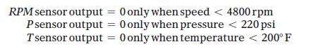
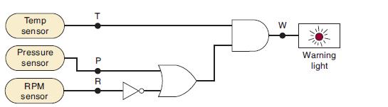
A jet aircraft employs a system for monitoring the rpm, pressure, and temperature values of its engines using sensors that operate as follows:Figure 3-56 shows the logic circuit that controls a cockpit warning light for certain combinations of engine conditions. Assume that a HIGH at output W
Show how a two-input NAND gate can be constructed from two-input NOR gates.
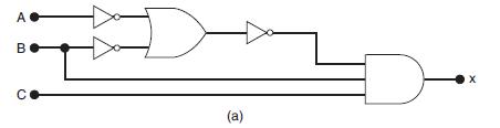
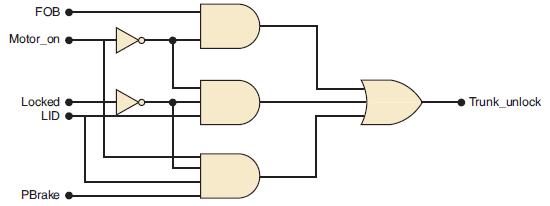
The trunk of an automobile is opened in one of two ways: by pressing a button on the trunk lid or by pressing the trunk button on the key fob. However, these buttons only open the trunk under certain conditions for safety and security purposes. The logic diagram for this circuit is shown in Figure
Show how a two-input NOR gate can be constructed from two-input NAND gates.
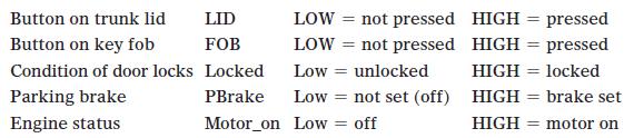
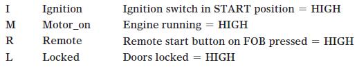
The remote start for an automobile will crank the engine under certain conditions. The logic circuit is shown in Figure 3-58. Inputs are defined as follows:(a) Write the Boolean expression from the circuit diagram.(b) Draw the truth table for this circuit.(c) Write the unsimplified SOP expression
For each statement below, draw the appropriate logic-gate symbol— standard or alternate—for the given operation.(a) A HIGH output occurs only when all three inputs are LOW.(b) A LOW output occurs when any of the four inputs is LOW.(c) A LOW output occurs only when all eight inputs are HIGH.
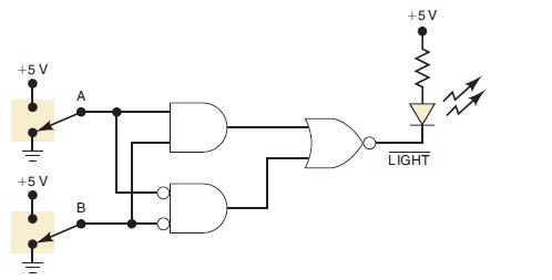
Modify the circuit of Figure 3-40 so that A1 = 0 is needed to produce LCD = 1 instead of A1 = 1.Figure 3-40 A₁ A₂ A3 A4 As As A7 A₂ IN OUT 74HC30 74HC02 W X Note: All gates are CMOS. 74HC32 74HC02 LCD
Draw the standard representations for each of the basic logic gates. Then draw the alternate representations.
Determine the input conditions needed to cause the output in Figure 3-59 to go to its active state.Figure 3-59 A B C DE E. X
(a) What is the asserted state for the output of Figure 3-59?(b) What is the asserted state for the output of Figure 3-36(c)?Figure 3-59Figure 3-36(c) A B C D Ш E X
Figure 3-60 shows an application of logic gates that simulates a two way switch like the ones used in our homes to turn a light on or off from two different switches. Here the light is an LED that will be ON (conducting) when the NOR gate output is LOW. Note that this output is labeledto indicate
Use the results of Problem 3-40 to obtain the complete truth table for the circuit of Figure 3-59.Data from Problem 3-40Determine the input conditions needed to cause the output in Figure 3-59 to go to its active state.Figure 3-59 A B C DE E. X
A 7406 TTL inverter has a maximum tPLH of 15 ns and a tPHL of 23 ns. A positive pulse that lasts 100 ns is applied to the input.(a) Draw the input and output waveforms. Scale the X-axis such that the end time is 200 ns.(b) Label tPLH and tPHL on the graph.(c) What is the pulse width of the output
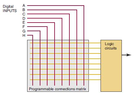
Redraw the programmable connection matrix from Figure 3-44. Label the output signals (horizontal lines) from the connection matrix (from top row to bottom row) as follows: AAABADHE. Draw an X in the appropriate intersections to short-circuit a row to a column and create these connections to the
True or false:(a) VHDL is a computer programming language.(b) VHDL can accomplish the same thing as AHDL.(c) AHDL is an IEEE standard language.(d) Each intersection in a switch matrix can be programmed as an open or short circuit between a row and column wire.(e) The first item that appears at the
Write the HDL code in the language of your choice that will produce the following output functions: X = A + B Y = AB Z = A + B + C
Refer to Figure 3-40 in Example 3-23. Inputs A7 through A0 are address inputs that are supplied to this circuit from outputs of the microprocessor chip in a microcomputer. The eight-bit address code A7 to A0 selects which device the microprocessor wants to activate. In Example 3-23, the required
Write the HDL code in the language of your choice that will implement the logic circuit of Figure 3-39.(a) Use a single Boolean equation.(b) Use the intermediate variables V, W, X, and Y.Figure 3-39 RD ROM-A ROM-B RAM X W V MEM
Show how x = ABC̅ can be implemented with one two-input NOR and one two-input NAND gate.
Implement y = ABCD using only two-input NAND gates.
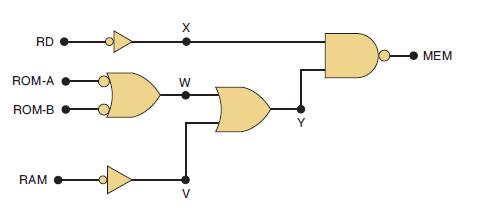
The output of the INVERTER of Figure 3-11 is connected to the input of a second INVERTER. Determine the output level of the second INVERTER for each level of input A.Figure 3-11 NOT A 0 1 | x = A 1 (a) A NOT x = A Presence of small circle always denotes inversion (b) A BL חד (c)
How many bytes are needed to represent 23510 in binary?
In Figure 3-15(a), change each AND gate to an OR gate, and change the OR gate to an AND gate. Then write the expression for output x.Figure 3-15(a) A KA А ABC A+ D A+ D x = ABC (A + D)
Use the expression for x to determine the output of the circuit in Figure 3-15(a) for the conditions A = 0, B = 1, C = 1, and D = 0.Figure 3-15(a) ABC D A ABC A+D (a) A+D x = ABC (A + D)
What is the designation used for intermediate signals?
Use the method of Examples 3-22 and 3-23 to determine the input conditions needed to activate the output of the circuit in Figure 3-37(b).Figure 3-37bData from example 3-22The logic circuit in Figure 3-39 generates an output, MEM, that is used to activate the memory ICs in a particular
Write the interpretation of the operation performed by the standard NOR gate symbol in Figure 3-33Figure 3-33 AND OR NAND NOR AC ве A B A B A B INV АС- O A B A+B KA AB A+B = A B A B A B A B A O KA А A+B=AB A B A+B A+B=AB A B=A+B
Draw the circuit diagram that implements the expressionusing gates with no more than three inputs. x = ABC(A + D)
What is the only set of input conditions that will produce a HIGH output from a three-input NOR gate?
Why are the transitions not vertical when measuring propagation delay?
Use theorems (13) and (14) to simplifyTheorem 13Theorem 14 y = AC + ABC.
Name five ways to describe the operation of logic circuits.
What does HDL stand for?
What does PLD stand for?
Showing 1300 - 1400
of 1612
First
3
4
5
6
7
8
9
10
11
12
13
14
15
16
17
Step by Step Answers
![P From D D transmitter Even-parity checker (b) Error (E) (1 = error 0= no error]](https://dsd5zvtm8ll6.cloudfront.net/images/question_images/1699/6/2/5/244654e391c6b1681699625247537.jpg)
![(MSB) A/D converter (LSB) Input port P1[7] P1 [6] P1[5] P1[4] P1[3] P1 [2] P1[1] P1[0] P1](https://dsd5zvtm8ll6.cloudfront.net/images/question_images/1699/6/2/5/870654e3b8ee63a81699625874756.jpg)
![Insert Coin Quarter Dime Nickel Logic Circuit D cents[4.00] N Five-bit array representing coin value](https://dsd5zvtm8ll6.cloudfront.net/images/question_images/1699/6/2/6/103654e3c77f15e11699626107828.jpg)
![A B O D E A+B (A + B)C (b) (A + B)C D + (A + B)C x = [D+ (A + B)C] E](https://dsd5zvtm8ll6.cloudfront.net/images/question_images/1699/5/9/8/479654dd08fbb7bb1699598482402.jpg)