New Semester
Started
Get
50% OFF
Study Help!
--h --m --s
Claim Now
Question Answers
Textbooks
Find textbooks, questions and answers
Oops, something went wrong!
Change your search query and then try again
S
Books
FREE
Study Help
Expert Questions
Accounting
General Management
Mathematics
Finance
Organizational Behaviour
Law
Physics
Operating System
Management Leadership
Sociology
Programming
Marketing
Database
Computer Network
Economics
Textbooks Solutions
Accounting
Managerial Accounting
Management Leadership
Cost Accounting
Statistics
Business Law
Corporate Finance
Finance
Economics
Auditing
Tutors
Online Tutors
Find a Tutor
Hire a Tutor
Become a Tutor
AI Tutor
AI Study Planner
NEW
Sell Books
Search
Search
Sign In
Register
study help
computer science
digital systems principles and application
Digital Systems Principles And Application 12th Edition Ronald Tocci, Neal Widmer, Gregory Moss - Solutions
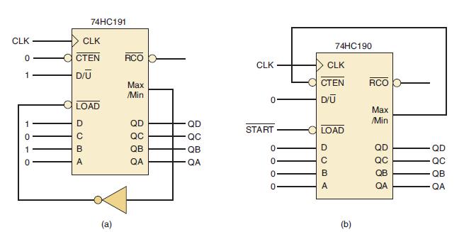
Refer to the IC counter circuit in Figure 7-107(a).(a) Draw the timing diagram for outputs QD QC QB QA.(b) What is the counter’s modulus?(c) What is the count sequence? Does it count up or down?(d) Can we produce the same modulus with a 74HC190? Can we produce the same count sequence with a
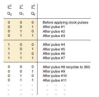
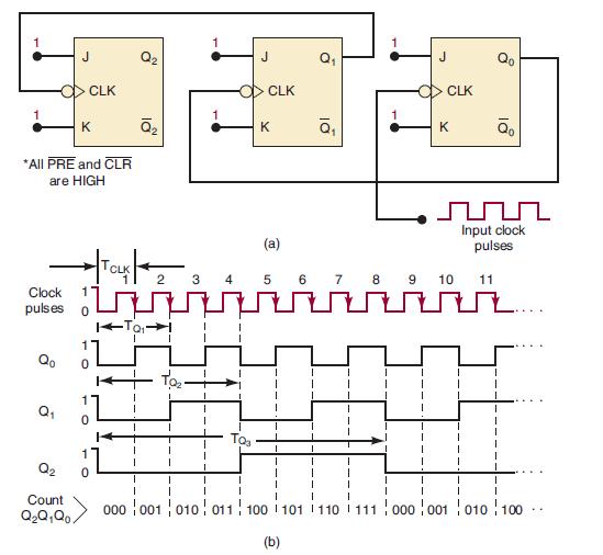
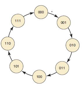
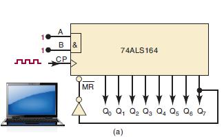
Assume that the initial contents of the 74ALS164 register in Figure 7-74(a) are 00000000. Determine the sequence of states as clock pulses are applied.Figure 7-74(a) A B& nnn CP MR 74ALS164 Qo Q₁ Q₂ Q3 Q4 Q5 Q6 Q7 (a)
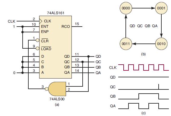
Figure 7-79(a) shows a 74ALS161 wired as a MOD-12 counter, but it produces the count sequence given in Figure 7-79(b). Determine the cause of the incorrect circuit behavior.Figure 7-79
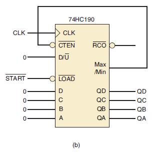
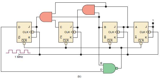
Refer to the IC counter circuit in Figure 7-107(b):(a) Describe the counter’s output on QD QC QB QA if S̅T̅A̅R̅T̅ is LOW.(b) Describe the counter’s output on QD QC QB QA if S̅T̅A̅R̅T̅ is momentarily pulsed LOW and then returns to a HIGH.(c) What is the counter’s modulus? Is this a
Draw a schematic to create a recycling, MOD-6 counter that produces the count sequence:(a) 1, 2, 3, 4, 5, 6, and repeats with a 74ALS162(b) 5, 4, 3, 2, 1, 0, and repeats with a 74ALS190(c) 6, 5, 4, 3, 2, 1, and repeats with a 74ALS190
Design a MOD-5 ring counter using LPM_SHIFTREG. Use an asynchronous control to restart the ring counter at 10000 so that it will begin counting in the proper sequence and include an active-HIGH count enable control.
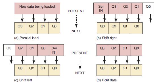
Suppose we want to design a universal four-bit shift register, using HDL, that has four synchronous modes of operation: Hold Data, Shift Left, Shift Right, and Parallel Load. Two input bits will select the operation that is to be performed on each rising edge of the clock. To implement a shift
Design a MOD-100, binary counter using either two 74HC161 or two 74HC163 chips and any necessary gates. The IC counter chips are to be synchronously cascaded together to produce the binary count sequence for 0 to 99. The MOD-100 is to have two control inputs, an active-LOW count enable (EN) and an
Design a MOD-100, BCD counter using either two 74HC160 or two 74HC162 chips and any necessary gates. The IC counter chips are to be synchronously cascaded together to produce the BCD count sequence for 0 to 99. The MOD-100 is to have two control inputs, an active-HIGH count enable (EN) and an
With a 6-MHz clock input to a 74ALS163 that has all four control inputs HIGH, determine the output frequency and duty cycle for each of the five outputs (including RCO).
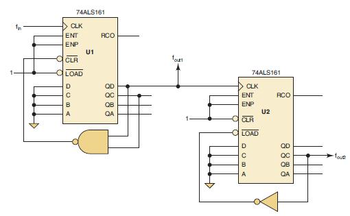
The frequency of fin is 6 MHz in Figure 7-108. The two IC counter chips have been cascaded asynchronously so that the output frequency produced by counter U1 is the input frequency for counter U2. Determine the output frequency for fout1 and fout2.Figure 7-108 fn 74ALS161 >
With a 6-MHz clock input to a 74ALS162 that has all four control inputs HIGH, determine the output frequency and duty cycle for each of the following outputs: QA, QC, QD, RCO. What is unusual about the waveform pattern that would be produced by the QB output? This pattern characteristic results in
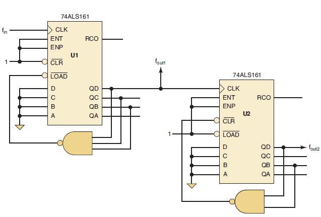
The frequency of fin is 1.5 MHz in Figure 7-109. The two IC counter chips have been cascaded asynchronously so that the output frequency produced by counter U1 is the input frequency for counter U2. Determine the output frequency for fout1 and fout2.Figure 7-109
Design a frequency divider circuit that will produce the following three output signal frequencies: 1.5 MHz, 150 kHz, and 100 kHz. Use 74HC162 and 74HC163 counter chips and any necessary gates. The input frequency is 12 MHz.
Design a frequency divider circuit that will produce the following three output signal frequencies: 1 MHz, 800 kHz, and 100 kHz. Use 74HC160 and 74HC161 counter chips and any necessary gates. The input frequency is 12 MHz.
Draw the AND gates necessary to decode the 10 states of the BCD counter of Figure 7-8(b).Figure 7-8(b) D D J CLKO K CLR 1 MHz с J CLK O C K CLR B B B J CLKO K CLR A K J CLK O CLR K
Draw the gates necessary to decode all of the states of a MOD-16 counter using active-LOW outputs.
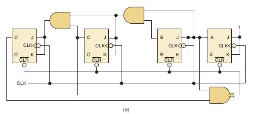
Analyze the synchronous counter in Figure 7-110(a). Draw its timing diagram and determine the counter’s modulus.Figure 7-110(a) D D CLK CLR O J CLK K с ē CLK O K CLR (a) B B J CLKO K CLR J CLKO K CLR
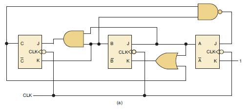
Analyze the synchronous counter in Figure 7-111(a). Draw its timing diagram and determine the counter’s modulus.Figure 7-111(a) C 10 J CLKO K CLK B 100 B J CLK O K (a) 14 J CLKO K
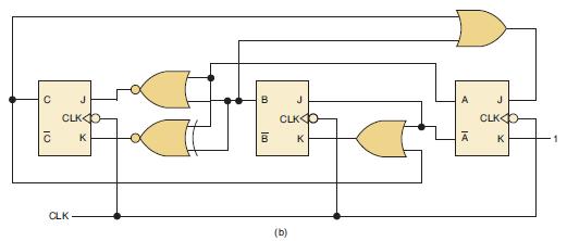
Repeat Problem 7-39 for Figure 7-111(b).Figure 7-111(b) B J CLKO inging K с CLKO- C K CLK (b) A 14 A J CLKO K 1
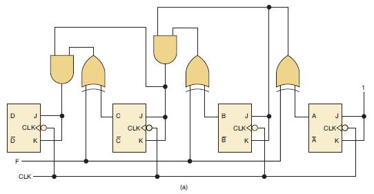
Analyze the synchronous counter in Figure 7-112(a). F is a control input. Draw its state transition diagram and determine the counter’s modulus.Figure 7-112(a) D 10 D F J CLKO K CLK o с C 3 CLKO K (a) B B J CLK O K A Ā L CLKO K
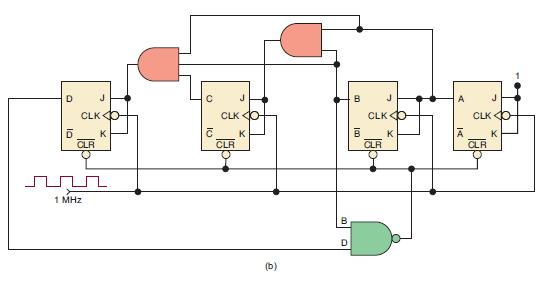
Analyze the synchronous counter in Figure 7-112(b). Draw its complete state transition diagram and determine the counter’s modulus. Is the counter self-correcting?Figure 7-112(b) с C 10 CLOCK > D CLK Dc B B Im B D CLK (b) Da A A D CLK
(a) Design a synchronous counter using J-K FFs that has the following sequence: 000, 010, 101, 110, and repeat. The undesired (unused) states 001, 011, 100, and 111 must always go to 000 on the next clock pulse.(b) Redesign the counter of part (a) without any requirement on the unused states; that
Design a synchronous, recycling, MOD-5 down counter that produces the sequence 100, 011, 010, 001, 000, and repeat. Use J-K flip-flops.(a) Force the unused states to 000 on the next clock pulse.(b) Use don’t-care NEXT states for the unused states. Is this design self-correcting?
Design a synchronous, recycling, BCD down counter with J-K FFs using don’t-care NEXT states.
Design a synchronous, recycling, MOD-7 up/down counter with J-K FFs. Use the states 000 through 110 in the counter. Control the count direction with input D (D = 0 to count up and D = 1 to count down).
Design a synchronous, recycling, MOD-8, binary down counter with D flip-flops.
Design a synchronous, recycling, MOD-12 counter with D FFs. Use the states 0000 through 1011 in the counter.
Design a recycling, MOD-13, up counter. The count sequence should be 0000 through 1100. Simulate (functional) the counter.(a) Use LPM_COUNTER.(b) Use an HDL.
Design a recycling, MOD-25, down counter. The count sequence should be 11000 through 00000. Simulate (functional) the counter.(a) Use LPM_COUNTER.(b) Use an HDL.
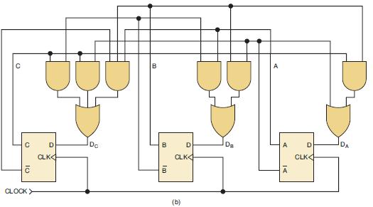
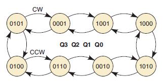
Design a bidirectional, half-step controller for a stepper motor using an HDL. The direction control input (dir) will produce a clockwise (CW) pattern when HIGH or counterclockwise when LOW. The sequence is given in Figure 7-113. Simulate the sequential circuit.Figure 7-113
Design a recycling, MOD-16 Gray code counter using an HDL. The counter should have an active-HIGH enable (cnt). Simulate the counter.
Design a frequency divider circuit to output a 100-kHz signal. The input frequency is 5 MHz. Simulate (functional) the counter.(a) Use LPM_COUNTER.(b) Use an HDL.
Design a frequency divider circuit that will output either of two specified frequency signals. The output frequency is selected by the control input fselect. The divider will output a frequency of 5 kHz when fselect = 0 or 12 kHz when fselect = 1. The input frequency is 60 kHz.Simulate (functional)
Expand the full-featured HDL counter to a MOD-256 counter. Simulate the counter.
Expand the full-featured HDL counter to a MOD-1024 counter. Simulate the counter.
Design a recycling, MOD-16, down counter. The counter should have the following controls (from lowest to highest priority): an active- LOW count enable (en), an active-HIGH synchronous clear (clr), and active-LOW synchronous load (ld). Decode the terminal count when enabled by en. Simulate
Design a recycling, MOD-10, up/down counter. The counter will count up when up = 1 and will count down when up = 0. The counter should also have the following controls (from lowest to highest priority): an active-HIGH count enable (enable), active-HIGH synchronous load (load), and an active-LOW
Create a MOD-1000 BCD counter by cascading together three of the HDL BCD counter modules . Simulate the counter.
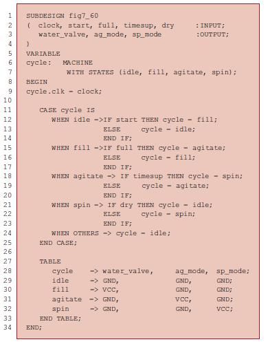
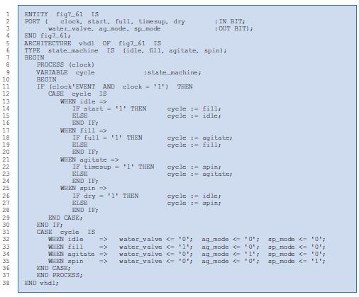
Modify the HDL description in Figure 7-60 or Figure 7-61 to add a rinse sequence after the clothes are washed. The new state machine sequence should be idle → wash_fill → wash_agitate → wash_spin → rinse_fill → rinse_agitate → rinse_spin → idle. Use hot water to wash, and cold water
Create a MOD-256 binary counter by cascading together two of the full-featured, MOD-16, HDL counter modules. Simulate the counter.
Design a synchronous, MOD-50 BCD counter by cascading a MOD-10 and a MOD-5 counter together. The MOD-50 counter should have an active-HIGH count enable (enable) and an active-LOW synchronous clear (clrn). Be sure to include the terminal count detection for the one’s digit to cascade with the
Design a synchronous, MOD-100, BCD down counter by cascading two MOD-10, down counter modules together. The MOD-100 counter should have a synchronous parallel load (load). Simulate (functional) the counter.(a) Use LPM_COUNTER.(b) Use an HDL.
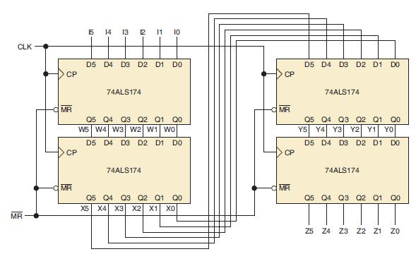
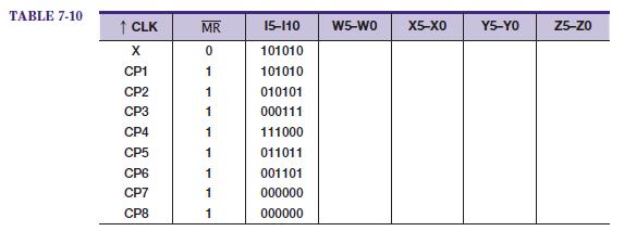
A set of 74ALS174 registers is connected as shown in Figure 7-114. What type of data transfer is performed with each register? Determine the output of each register when the M̅R̅ is pulsed momentarily LOW and after each of the indicated clock pulses (CP#) in Table 7-10. How many clock pulses must
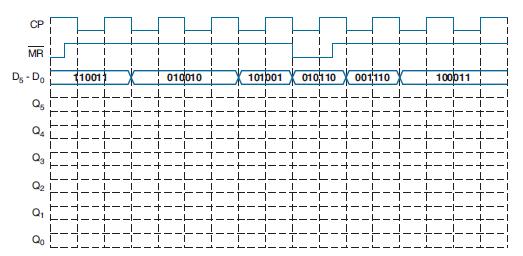
Complete the timing diagram in Figure 7-115 for a 74HC174. How does the timing diagram show that the master reset is asynchronous?Figure 7-115 MR 8 8 d ♂ ♂ ģ 8 1 1001 I T T 1 010010 I T 1 101001 010110 T T 001110 1 1 T T 100011 II I
Simulate the HDL traffic light controller design presented.
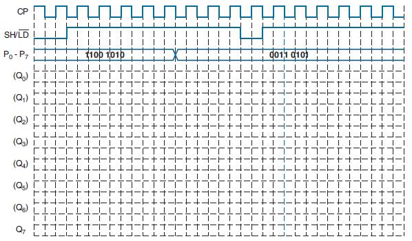
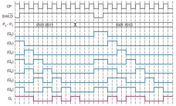
Repeat Example 7-22 with DS = 1 and the input waveforms given in Figure 7-117.Figure 7-117Data from Example 7-22Determine the output signal at Q7 if we connect a 74HC165 with DS = 0 and CP INH = 0 and then apply the input waveforms given in Figure 7-72. P0 – P7 represent the parallel data on P0
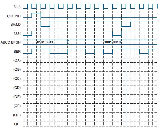
Apply the input waveforms given in Figure 7-118 to a 74ALS166 and determine the output produced.Figure 7-118 CLK CLK INH SH/LD CLR ABCD EFGH SER (QA) (QB) (QC) (QD) (QE) (QF) (QG) QH F+ LIL. +-+- ודז 01010011 +--- +1- 10010010 | | 1 PE -FT +-1 -F -ד 다. ++-++-++-- TOTOSITIC
How many clock pulses will be needed to completely load eight bits of serial data into a 74ALS166? How does this relate to the number of flip-flops contained in the register?
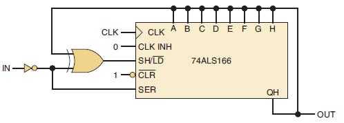
While examining the schematic for a piece of equipment, a technician or an engineer will often come across an IC that is unfamiliar. In such cases, it is often necessary to consult the manufacturer’s data sheets for specifications on the device. Research the data sheet for the 74AS194
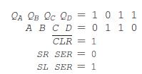
Refer to Figure 7-119 to answer the following questions:(a) Which register function (load or shift) will be performed on the next clock if in = 1 and out = 0? What data value will be input when clocked?(b) Which register function (load or shift) will be performed on the next clock if in = 0 and out
Draw the diagram for a MOD-5 ring counter using J-K flip-flops. Make sure that the counter will start the proper count sequence when it is turned on.
Add one more J-K flip-flop to convert the MOD-5 ring counter in Problem 7-73 into a MOD-10 counter. Determine the sequence of states for this counter. This is an example of a decade counter that is not a BCD counter. Draw the decoding circuit for this counter.Data from Problem 7-73Draw the diagram
The MOD-10 counter in Figure 7-8(b) produces the count sequence 0000, 0001, 0010, 0011, 0100, 0101, 0110, 0111, and repeats. Identify some possible fault conditions that might produce this result.Figure 7-8(b) D D J CLK O K CLR O 1 MHz с 10 J CLK CLR K (b) B B 100 B J CLKO K CLR 14 J CLK O CLR K
Draw the diagram for a MOD-10 Johnson counter using a 74HC164. Make sure that the counter will start the proper count sequence when it is turned on. Determine the count sequence for this counter and draw the decoding circuit needed to decode each of the 10 states. This is another example of a
The clock input to the Johnson counter in Problem 7-75 is 10 Hz. What is the frequency and duty cycle for each of the counter outputs?Data from Problem 7-75Draw the diagram for a MOD-10 Johnson counter using a 74HC164. Make sure that the counter will start the proper count sequence when it is
The MOD-10 counter in Figure 7-8(b) produces the count sequence 0000, 0101, 0010, 0111, 1000, 1101, 1010, 1111, and repeats. Identify some possible fault conditions that might produce this result.Figure 7-8(b) D D J CLK O K CLR O 1 MHz с 10 J CLK CLR K (b) B B 100 B J CLKO K CLR 14 J CLK O CLR K
Create an eight-bit SISO shift register. The serial input is called ser and the serial output is called qout. An active-LOW enable (en) controls the shift register. Simulate (functional) the design.(a) Use LPM_SHIFTREG. Use any necessary logic gates.(b) Use an HDL.
Create an eight-bit PIPO shift register. The data in is d[7..0] and the outputs are q[7..0]. An active-HIGH enable (ld) controls the shift register.Simulate (functional) the design.(a) Use LPM_FF.(b) Use an HDL.
Create an eight-bit PISO shift register. The data in is d[7..0] and the output is q0. The shift-register function is controlled by sh_ld 1sh_ld = 0 to synchronously parallel load and sh_ld = 1 to serial shift). The serial input while shifting should be a constant LOW. The register also should have
Create an eight-bit SIPO shift register. The data in is ser_in and the outputs are q[7..0]. The shift-register function is enabled by an active-HIGH control named shift. The shift register also has a higher priority active-HIGH synchronous clear (clear). Simulate (functional) the design.(a) Use
Design a MOD-10, self-starting Johnson counter with an active-HIGH, asynchronous reset (reset) using an HDL. Simulate the design.
Use Altera’s simulator to test the nonretriggerable, level-sensitive, one-shot design example in either Figure 7-95 (AHDL) or 7-96 (VHDL). Use a 1-kHz clock and create a 10-ms output pulse for the simulation. Verify that:(a) The correct pulse width is created when triggered.(b) The output can be
Sometimes a digital application may need a ring counter that recirculates a single zero instead of a single one. The ring counter would then have an active-LOW output instead of an active-HIGH. Design a MOD-8, self-starting ring counter with an active-LOW output using an HDL. The ring counter
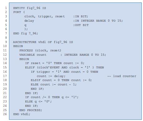
Modify the nonretriggerable, level-sensitive, one-shot design example from either Figure 7-95 (AHDL) or Figure 7-96 (VHDL) so that the one-shot is retriggerable but still level-sensitive. Simulate the design.Figure 7-95Figure 7-96 12345 6 7 8 9 SUBDESIGN fig7_95 ( ) clock, trigger, reset delay
For each of the following statements, indicate the type(s) of counter being described.(a) Each FF is clocked at the same time.(b) Each FF divides the frequency at its CLK input by 2.(c) The counting sequence is 111, 110, 101, 100, 011, 010, 001, 000.(d) The counter has 10 distinct states.(e) The
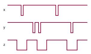
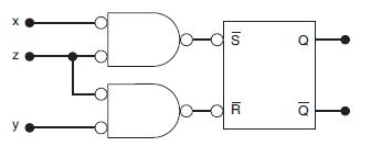
Invert the x and y waveforms of Figure 5-87, apply them to the SET and RESET inputs of a NOR latch, and determine the Q and Q̅ waveforms. Assume that Q = 0 initially.Figure 5-87 X Z ㅠ ㅜ
The waveforms of Figure 5-87 are connected to the circuit of Figure 5-88. Assume that Q = 0 initially, and determine the Q waveform.Figure 5-87Figure 5-88 X Z ㅠ ㅜ
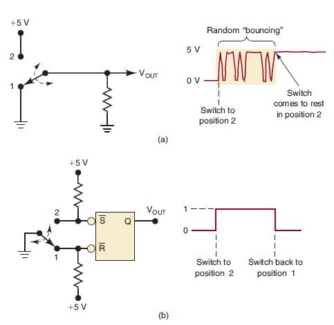
Modify the circuit of Figure 5-9 to use a NOR gate latch.Figure 5-9 +5 V 2 +5 V +5 V www S R O VOUT (a) VOUT (b) 5 V ov 1 0 Random "bouncing" Switch to position 2 Switch to position 2 Switch comes to rest in position 2 Switch back to position 1
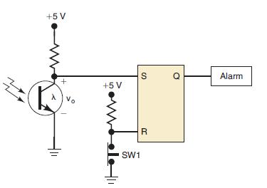
Modify the circuit of Figure 5-12 to use a NAND gate latch.Figure 5-12 +5 V +5 V S R SW1 Q Alarm
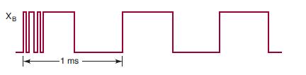
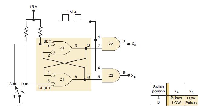
Refer to the circuit of Figure 5-13. A technician tests the circuit operation by observing the outputs with a storage oscilloscope while the switch is moved from A to B. When the switch is moved from A to B, the scope display of XB appears as shown in Figure 5-89. What circuit fault could produce
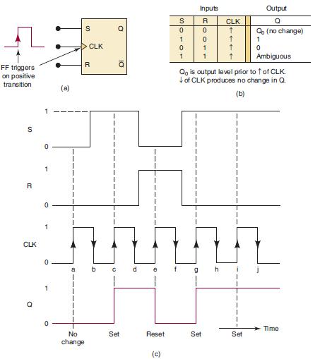
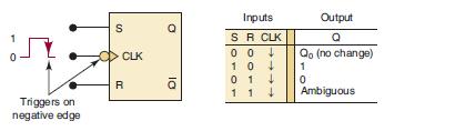
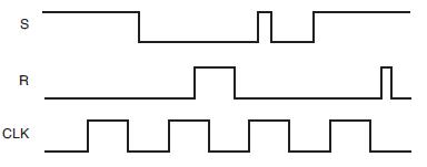
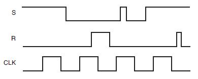
Apply the S, R, and CLK waveforms of Figure 5-20 to the FF of Figure 5-21, and determine the Q waveform.Figure 5-20Figure 5-21 FF triggers on positive transition S R CLK O 1 0 0 1 0 0 (a) S CLK R No change O 10 Set Reset (c) S 010 Inputs ROOT 0 Set 1 1 CLK t ↑ ↑ ↑ 1 Ambiguous Qo is output
A certain clocked FF has minimum tS = 20 ns and tH = 5 ns. How long must the control inputs be stable prior to the active clock transition?
Apply the waveforms of Figure 5-90 to the FF of Figure 5-20 and determine the waveform at Q. Repeat for the FF of Figure 5-21. Assume Q = 0 initially.Figure 5-90Figure 5-20Figure 5-21 S R CLK JL
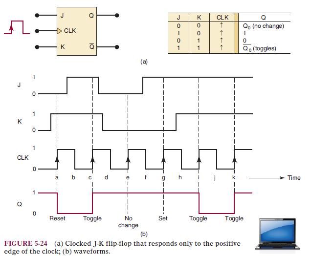
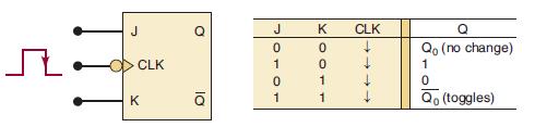
Apply the J, K, and CLK waveforms of Figure 5-24 to the FF of Figure 5-25. Assume that Q = 1 initially, and determine the Q waveform.Figure 5-24Figure 5-25 K CLK 1 0 O 1 0 1 0 J CLK K O 10 a b c d Reset Toggle I No change (a) J 1000 Set 1 gh XOO K 0 1 Toggle CLK j Qo (no change) (b) FIGURE 5-24 (a)
Draw the following digital pulse waveforms. Label tr, tf, and tw, leading edge, and trailing edge.(a) A negative TTL pulse with tr = 20 ns, tf = 5 ns, and tw = 50 ns.(b) A positive TTL pulse with tr = 5 ns, tf = 1 ns, and tw = 25 ns.(c) A positive pulse with tw = 1 ms whose leading edge occurs
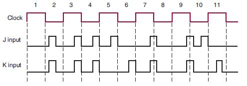
The waveforms shown in Figure 5-91 are to be applied to two different FFs:(a) Positive-edge-triggered J-K(b) Negative-edge-triggered J-KDraw the Q waveform response for each of these FFs, assuming that Q = 0 initially. Assume that each FF has tH = 0.Figure 5-91 Clock Jinput K input 1 2 3 4 5 6 7 8
(a) Show how a J-K flip-flop can operate as a toggle FF (changes states on each clock pulse). Then apply a 10-kHz clock signal to its CLK input and determine the waveform at Q.(b) Connect Q from this FF to the CLK input of a second J-K FF that also has J = K = 1. Determine the frequency of the
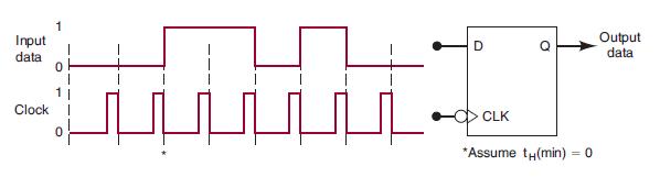
A D FF is sometimes used to delay a binary waveform so that the binary information appears at the output a certain amount of time after it appears at the D input.(a) Determine the Q waveform in Figure 5-92, and compare it with the input waveform. Note that it is delayed from the input by one clock
(a) Apply the S and CLK waveforms of Figure 5-90 to the D and CLK inputs of a D FF that triggers on PGTs. Then determine the waveform at Q.(b) Repeat using the C waveform of Figure 5-90 for the D input.Figure 5-90 S R CLK n L
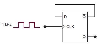
An edge-triggered D flip-flop can be made to operate in the toggle mode by connecting it as shown in Figure 5-93. Assume that Q = 0 initially, and determine the Q waveform.Figure 5-93 1 kHz D CLK 10 Q
(a) Apply the S and CLK waveforms of Figure 5-90 to the D and EN inputs of a D latch, respectively, and determine the waveform at Q.(b) Repeat using the C waveform applied to D.Figure 5-90 S R CLK n L
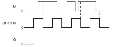
Compare the operation of the D latch with a negative-edge-triggered D flip-flop by applying the waveforms of Figure 5-94 to each and determining the Q waveforms.Figure 5-94 D CLK/EN Q 0 0 0 ㄴ 머
In Problem 5-16, we saw how an edge-triggered D flip-flop can be operated in the toggle mode. Explain why this same idea will not work for a D latch.Data from Problem 5-16An edge-triggered D flip-flop can be made to operate in the toggle mode by connecting it as shown in Figure 5-93. Assume that Q
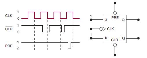
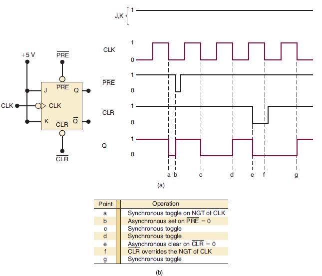
Determine the Q waveform for the FF in Figure 5-95. Assume that Q = 0 initially, and remember that the asynchronous inputs override all other inputs.Figure 5-95 CLK CLR PRE 1 0 1 0 1 1 J PRE CLK K CLR O Q
Apply the CLK, P̅R̅E̅, and C̅L̅R̅ waveforms of Figure 5-33 to a positiveedge-triggered D flip-flop with active-LOW asynchronous inputs. Assume that D is kept HIGH and Q is initially LOW. Determine the Q waveform.Figure 5-33
Apply the waveforms of Figure 5-95 to a D flip-flop that triggers on NGTs and has active-LOW asynchronous inputs. Assume that D is kept LOW and that Q is initially HIGH. Draw the resulting Q waveform.Figure 5-95 CLK CLR PRE 1 0 1 0 1 1 J PRE CLK K CLR O Q
Use the Texas Instrument website to look up the 74ALS74A DFF.(a) How long can it take for the Q output of a 74ALS74A to switch from 0 to 1 in response to an active CLK transition?(b) How long does the D input need to be stable before the active clock edge on the 74ALS74A?(c) What is the narrowest
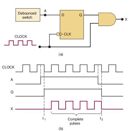
Modify the circuit of Figure 5-39 to use a J-K flip-flop.Figure 5-39 CLOCK snm CLOCK A Debounced switch X A 1 1 D (a) (b) CLK Q S Complete pulses L X
Use the Texas Instrument website to look up the 74ALS112A DFF.(a) How long does it typically take to asynchronously clear a 74ALS112?(b) How long maximum does it take to asynchronously set a 74ALS112?(c) What is the shortest acceptable interval between active clock transitions for a 74ALS74A?(d)
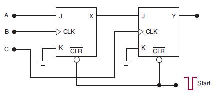
In the circuit of Figure 5-96, inputs A, B, and C are all initially LOW. Output Y is supposed to go HIGH only when A, B, and C go HIGH in a certain sequence.(a) Determine the sequence that will make Y go HIGH.(b) Explain why the START pulse is needed.(c) Modify this circuit to use D FFs.Figure 5-96
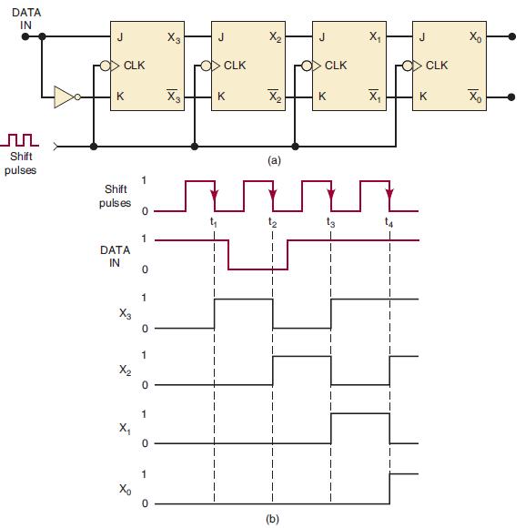
A recirculating shift register is a shift register that keeps the binary information circulating through the register as clock pulses are applied. The shift register of Figure 5-46 can be made into a circulating register by connecting flip-flop X0 to the DATA IN line. No external inputs are used.
(a) Draw a circuit diagram for the synchronous parallel transfer of data from one three-bit register to another using J-K flip-flops.(b) Repeat for asynchronous parallel transfer.
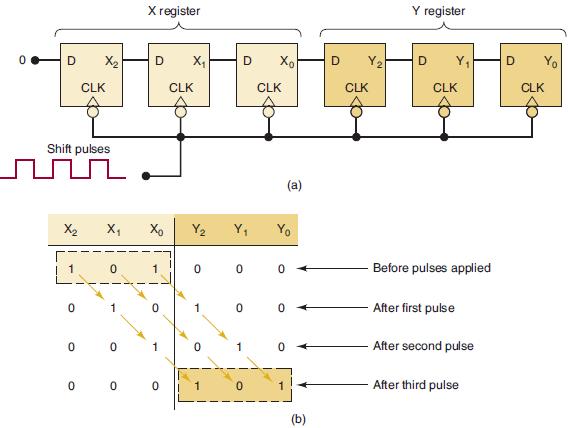
Refer to Figure 5-47, where a three-bit number stored in register X is serially shifted into register Y. How can the circuit be modified so that, at the end of the transfer operation, the original number stored in X is present in both registers?Figure 5-47 D X₂ Shift pulses 0 CLK X₂
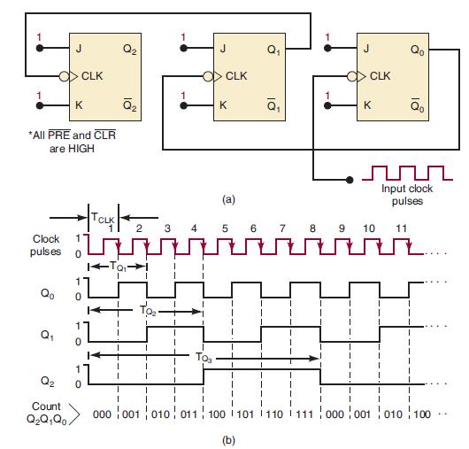
Refer to the binary counter of Figure 5-48. Change it by connecting X̅0 to the CLK of flip-flop X1, and X̅1 to the CLK of flip-flop X2. Start with all FFs in the 1 state, and draw the various FF output waveforms (X0, X1, X2,) for 16 input pulses. Then list the sequence of FF states as was done in
Refer to the counter circuit of Figure 5-48 and answer the following:(a) If the counter starts at 000, what will be the count after 13 clock pulses? After 99 pulses? After 256 pulses?(b) If the counter starts at 100, what will be the count after 13 pulses? After 99 pulses? After 256 pulses?(c)
Draw the state transition diagram for this down counter, and compare it with the diagram of Figure 5-50. How are they different?Figure 5-50 110 111 101 000 100 001 011 010
(a) How many FFs are required to build a binary counter that counts from 0 to 1023?(b) Determine the frequency at the output of the last FF of this counter for an input clock frequency of 2 MHz.(c) What is the counter’s MOD number?(d) If the counter is initially at zero, what count will it hold
A binary counter is being pulsed by a 256-kHz clock signal. The output frequency from the last FF is 2 kHz.(a) Determine the MOD number.(b) Determine the counting range.
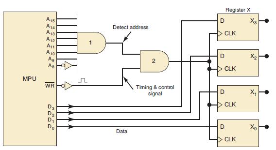
Modify the circuit of Figure 5-58 so that only the presence of address code 10110110 will allow data to be transferred to register X.Figure 5-58 MPU A15 A14 A13 A12 A11 A 10 Ag As WR D3 Л Detect address Data 2 Timing & control signal D D D D Register X CLK CLK CLK CLK X3 X₂ X₂ Xo
Showing 900 - 1000
of 1612
First
3
4
5
6
7
8
9
10
11
12
13
14
15
16
17
Step by Step Answers
![12345 6 7 8 9 SUBDESIGN fig7_95 ( ) clock, trigger, reset delay [3..0] q VARIABLE count [3..0] BEGIN 10 11 12](https://dsd5zvtm8ll6.cloudfront.net/images/question_images/1699/9/6/3/7886553638c8cef91699963788806.jpg)