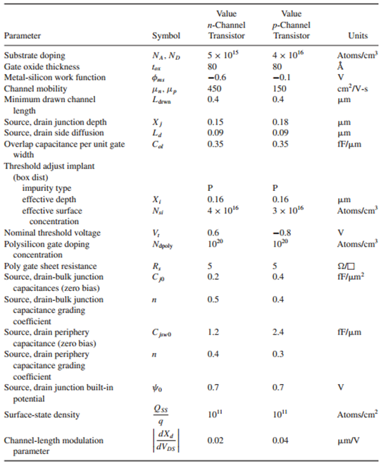
New Semester
Started
Get
50% OFF
Study Help!
--h --m --s
Claim Now
Question Answers
Textbooks
Find textbooks, questions and answers
Oops, something went wrong!
Change your search query and then try again
S
Books
FREE
Study Help
Expert Questions
Accounting
General Management
Mathematics
Finance
Organizational Behaviour
Law
Physics
Operating System
Management Leadership
Sociology
Programming
Marketing
Database
Computer Network
Economics
Textbooks Solutions
Accounting
Managerial Accounting
Management Leadership
Cost Accounting
Statistics
Business Law
Corporate Finance
Finance
Economics
Auditing
Tutors
Online Tutors
Find a Tutor
Hire a Tutor
Become a Tutor
AI Tutor
AI Study Planner
NEW
Sell Books
Search
Search
Sign In
Register
study help
physics
analysis and design integrated circuits
Analysis and Design of Analog Integrated Circuits 5th edition Paul R. Gray, Paul J. Hurst Stephen H. Lewis, Robert G. Meyer - Solutions
Repeat Problem 7.3 for the MOS circuit in Problem 7.2.Data from Prob. 7.3:Calculate an expression for the output impedance of the circuit in Problem 7.1 as seen by RL and form an equivalent circuit. Plot the magnitude of this impedance on log scales from f = 1 kHz to f = 100 MHz.Circuit in Prob.
Repeat Problem 7.3 for RS= 0 and RS= ˆž.Data from Prob. 7.3:Calculate an expression for the output impedance of the circuit in Problem 7.1 as seen by RL and form an equivalent circuit. Plot the magnitude of this impedance on log scales from f = 1 kHz to f = 100 MHz.Circuit in Prob. 7.1:
Calculate an expression for the output impedance of the circuit in Problem 7.1 as seen by RL and form an equivalent circuit. Plot the magnitude of this impedance on log scales from f = 1 kHz to f = 100 MHz.Circuit in Prob. 7.1: RL Vo Rs Vi Он
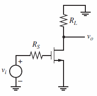
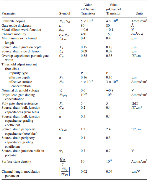
Repeat Problem 7.1 for the MOS commonsource stage shown in Fig. 7.2b using RS= 10 kΩ, RL= 5 kΩ, ID= 0.5 mA, and the following NMOS transistor data: NMOS: W = 100 µm, Ldrwn= 2 µm, Ld= 0.2 µm, Xd= 0, λ = 0, k€™n= 60 µA/V2,
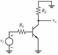
(a) Use the Miller approximation to calculate the ˆ’3-dB frequency of the small-signal voltage gain of a common-emitter transistor stage as shown in Fig. 7.2a using RS= 5 kΩ, RL= 3 kΩ, and the following transistor parameters: rb= 300 Ω, IC= 0.5 mA,
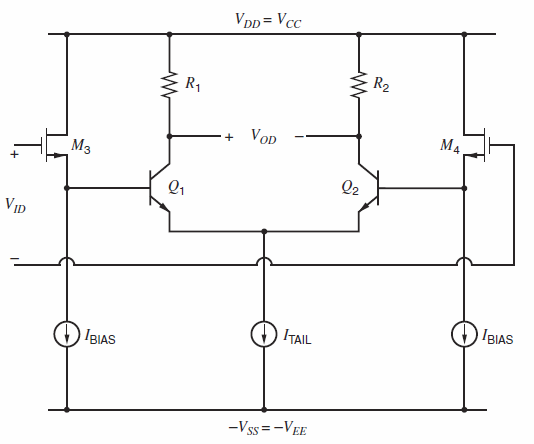
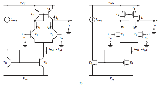
In BiCMOS technology, MOS source followers can be used to drive a bipolar differential pair to reduce the average current flowing in the stage input leads. See Fig. 6.64. Calculate the input-referred random offset voltage of this structure. Assume nonzero mismatch occurs in the following
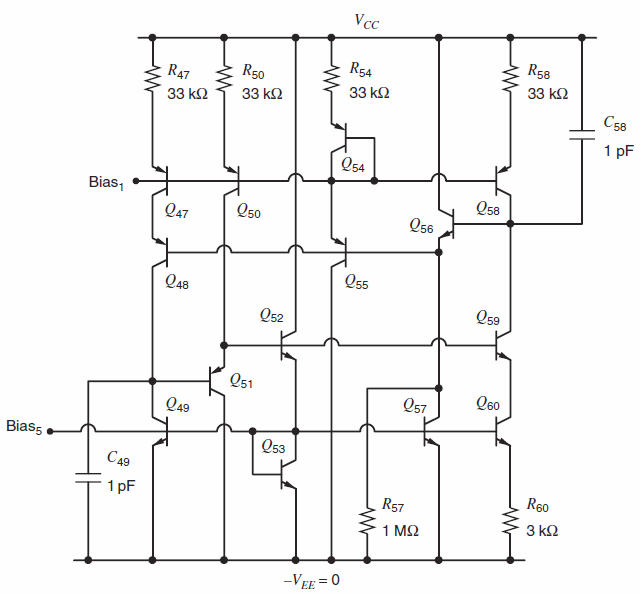
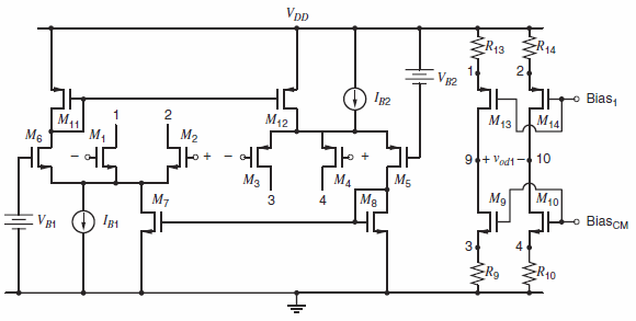
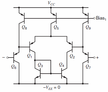
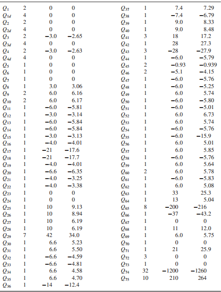
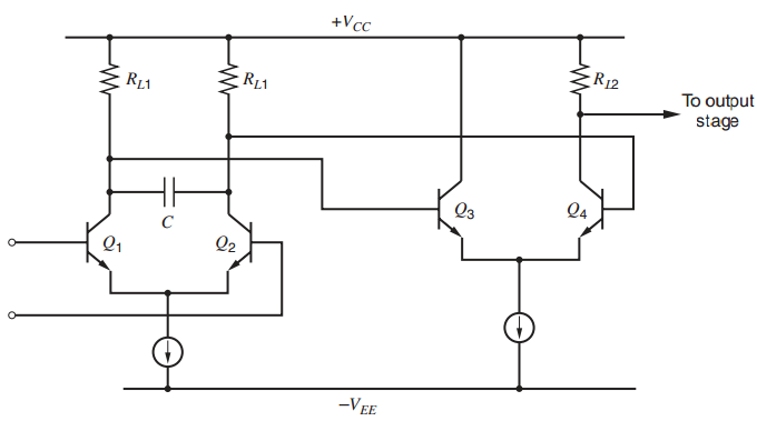
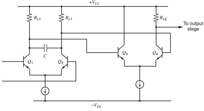
Find the minimum value of VCC for proper operation of the NE5234 op amp. For simplicity, assume VEE= 0, |VBE(on)| = 0.7 V, and |VCE(sat)| = 0.1 V. Also, ignore base currents. Assume the bias circuits in Figures 6.34 and 6.40 operate properly even though some transistors in these circuits may
(a) Suppose that the npn and pnp transistors in the input stage of the NE5234 op amp are changed into n-channel and p-channel MOS transistors, respectively. If transistors conducting nonzero current operate in strong inversion, the transconductance of the revised circuit depends on the common-mode
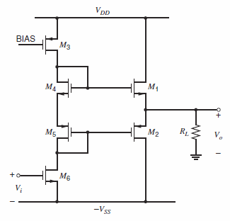
Repeat Problem 6.29 except replace each pnp transistor with a p-channel MOS transistor and replace each npn transistor with an n-channel MOS transistor. Assume Vt= 0.5 V and Vov= 0.1 V for all n-channel MOS transistors. Also, assume Vt= ˆ’ 0.5 V and Vov= ˆ’ 0.1 V for all
Find the small-signal voltage gain of the NE5234 op amp under the same conditions given in this chapter except use βF(npn) =β0(npn) = 80 and βF(pnp) = β0(pnp) = 20. Ignore βF(npn) and βF(pnp) from dc bias calculations except in calculating revised estimates of IC64, |IC65|, and IC68, as at
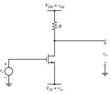
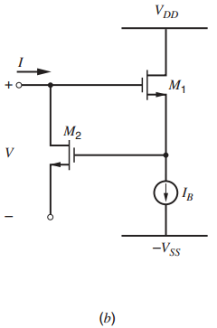
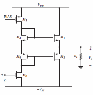
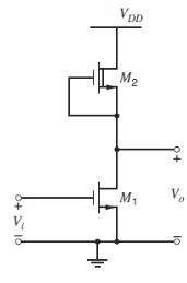
Calculate the low-frequency PSRR from the Vdd andVss power supplies for the common-source amplifier shown in Fig. 6.57. Assume the transistor is biased in the active region.Figure 6.57 VDD + Vdd ER Vo Vi Vss + Vss
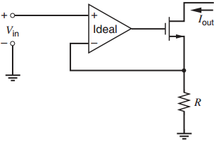
For the circuit of Fig. 6.53, determine the output current as a function of the input voltage. Assume that the transistor operates in the active region.Figure 6.53 lout Ideal Vin
In Fig. 6.31b, resistive loads were used to extend the common-mode input range to include ˆ’VEE. Fig. 6.62 shows another circuit with this characteristic. Find the common-mode range of this circuit. Assume that VBE(on)= 0.7 V and VCE(sat)= 0.1 V for the npn transistors. Also, assume that
Determine the small-signal voltage gain of the NE5234 if all the values of all the resistors in the input stage are doubled. Assume the common-mode input voltage is low enough that Q1 and Q2 are off. Assume the output stage is biased as described in this chapter.
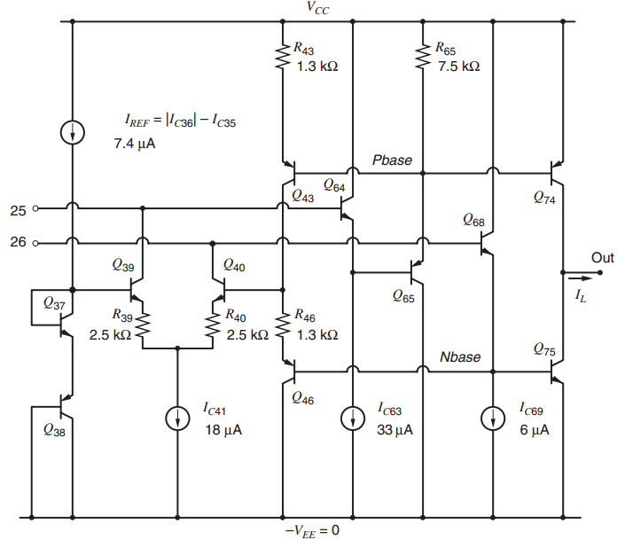
Fig. 6.61 shows an alternate scheme for biasing the NE5234 output stage.Ignoring all base currents, find |IC74| IC75. Use Fig. 6.42 for the relative emitter areas of all the transistors except assume that Q46 is identical to Q43.Figure 6.61Figure 6.42 Vcc R65 R43 7.5 k2 1.3 k2 IREF = |!c36l
Assume that Q75 does not saturate and calculate the maximum value of IC75 in the NE5234 op amp. Assume VEB70(on) = 0.7 V, IS71 = 6 × 10⁻¹⁸ A and IS75 = 6×10⁻¹⁷ A.
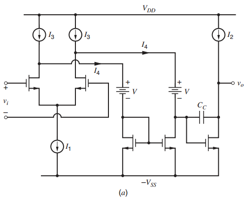
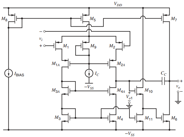
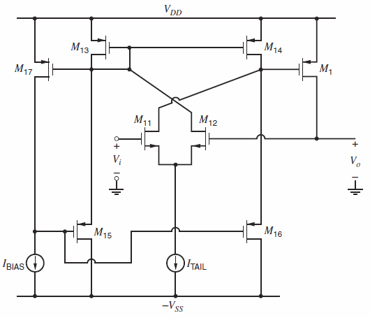
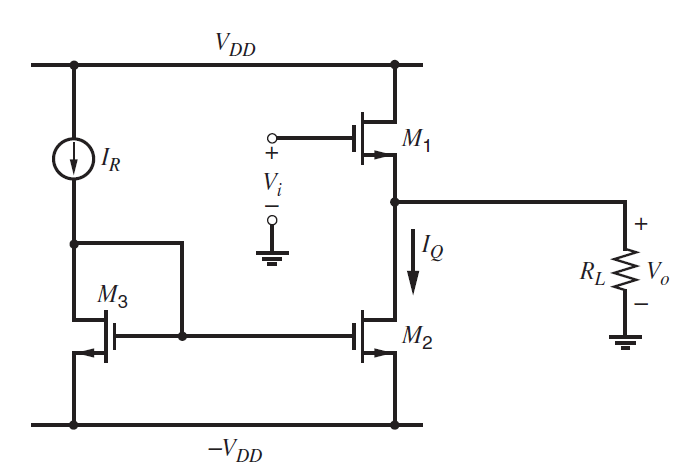
(a)Figure 6.60a shows a folded version of the op amp in Fig. 6.15. A differential inter stage level-shifting network composed of voltage sources V has been inserted between the first and second stages. Assume that current source I1is implemented using an n-channel transistor with overdrive of
Suppose that the peak-peak output swing requirement in Problem 6.22 is reduced while the other conditions are held constant. This change allows the overdrive magnitude to be increased. Which transistor in the bias circuit of Fig. 6.30d enters the triode region first if the overdrive magnitudes are
For the folded-active-cascode op amp in Fig. 6.30, choose the device sizes to give a peak-peak output swing of at least 2.5 V. Use the 0.4 μm CMOS model parameters in Table 2.4 except let γ = 0.25 V½and Xd= 0 for all transistors and Vt0= 0.7 V and ˆ’0.7 V
Draw the schematic of a folded-cascode op amp similar to the op amp in Fig. 6.28 except with two layers of both n- and p-type cascodes. Choose a current mirror that maximizes the output swing. Assume that all transistors have equal overdrive magnitudes except where changes are needed to maximize
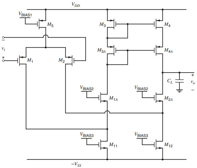
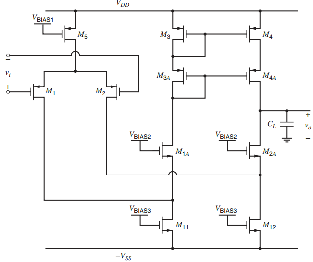
Design a CMOS op amp based on the folded-cascode architecture of Fig. 6.28 using supply voltages of ± 1.5 V. Use the bias circuit of Fig. 4.42 (with M3and M4cascoded) to generate the bias current IBIAS. Then design an extension to this bias circuit thatproduces the bias
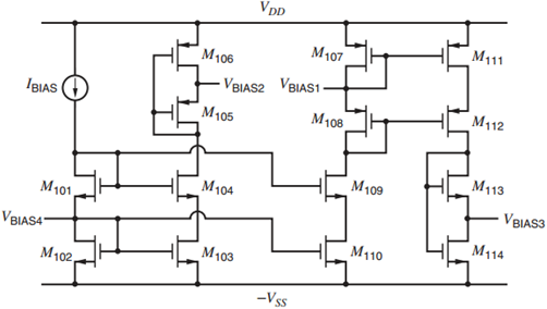
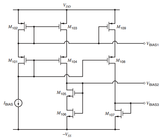
Find the low-frequency voltage gain from variation on each power supply to the op-amp out-put in Fig. 6.28. Assume that the bias voltages VBIAS1, VBIAS2, and VBIAS3are produced by the circuit shown in Fig. 6.59, where M106 is the only transistor that operates in the triode region. Assume that
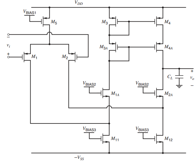
Calculate the common-mode input range of the folded-cascode op amp in Fig. 6.28. Assume that all the transistors are enhancement-mode devices with |Vt|=1 V, and ignore the body effect. Also assume that the biasing is arranged so that |Vov|=0.2 V for each transistor. Finally, assume that M11and
Draw a telescopic-cascode op amp similar to the first stage in Fig. 6.25 except use an n-channel input pair and a high-swing p-type cascode current-mirror load. Calculate the maximum output swing in terms of the common-mode input voltage. Deter-mine the optimum common-mode input voltage for
Calculate the common-mode input range of the op amp in Fig. 6.25. Assume that all the transistors are enhancement-mode devices with |Vt| = 1V,and ignore the body effect. Also assume that the biasing is arranged so that |Vov|=0.2 V for each transistor except M9. Finally, assume that M1and M2are
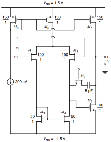
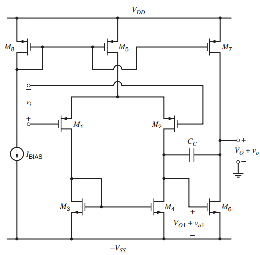
Calculate bias currents and the low-frequency small-signal voltage gain for the CMOS op amp of Fig. 6.58. Use the parameters given in Table 2.4, and assume that Xd=0.1 μm and dXd/dVDS = 0.04 μm/V for all the transistors at the operating point. Calculate the input
List and explain at least three reasons to select a two-stage op amp with an n-channel input pair instead of with a p-channel input pair for a given application.
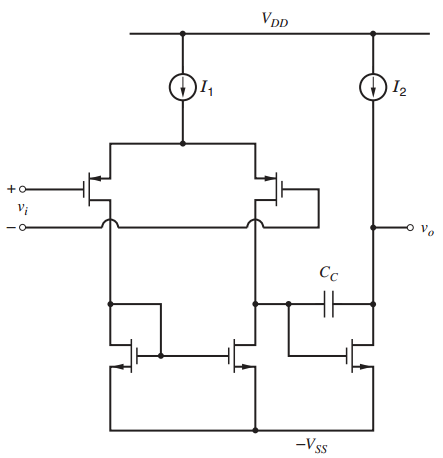
(a) Calculate the random input offset voltage for the op amp in Fig. 6.16. Assume the matching is perfect except thatVt3ˆ’Vt4= 10mV. Also assume that all transistors have equal W/Land operate in the active region. Ignore short-channel effects and use the data in Table 2.4.(b) Repeat (a)
(a) Equation 6.69 gives the random input off-set voltage of the op amp in Fig. 6.16. Explain the polarity of each term in (6.69) by assuming that the matching is perfect except for the term under consideration. Keep in mind that the overdrive is negative for p-channel transistors. Therefore, (6.69)
Draw a two-stage op amp similar to the op amp in Fig. 6.16 except reverse the polarity of every transistor. For example, the resulting op amp should have an n.-channel input pair. Calculate the following parameters: (a) Low-frequency voltage gain, (b) Output swing, (c) Systematic
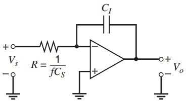
(a) Calculate and sketch the output voltage waveform of the switched-capacitor integrator of Fig. 6.10a from t =0 to t =20 μs assuming a fixed Vs = 1 V and a clock rate of 1 MHz. Assume an ideal MOS op amp with infinite gain and zero output rise time. Assume ideal MOS switches with
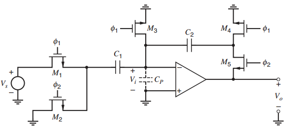
In the switched-capacitor amplifier of Fig. 6.9a, assume that the source of M4is connected to VSinstead of to ground. Calculate the output volt-age that appears during φ2for a given VS. Assume the op amp is ideal except that it has a finite gain a and a nonzero input capacitance CP.
Suppose an op amp with PSRR+= 10 is con-nected in the voltage-follower configuration shown in Fig. 6.3c. The input VSis set to zero, but a low- fre-quency ac signal with peak magnitude Vsup=20 mV is superimposed on the positive power supply. Calcu-late the peak magnitude of the output
Consider the differential amplifier shown in Fig. 6.4. Choose values of R1and R2for which the gain is equal toˆ’10 and the magnitude of the dc output voltage is less than or equal toˆ’10 mV with V1= V2= 0. Assume that the op amp is ideal except that |IOS|=100 nA.Figure 6.4 12 R2
Once the offset voltage of the differential amplifier in Problem 6.4 is adjusted to zero, the input-referred offset voltage must remain less than 1 mV in magnitude for common-mode input voltages between ± 10 V. What is the minimum CMRR allowable for the amplifier to meet this
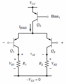
The differential instrumentation amplifier shown in Fig. 6.56 must have a voltage gain of 103 with an accuracy of 0.1 percent. What is the minimum required open-loop gain of the op amp? Assume the op amp open-loop gain has a tolerance of +100 percent, 50 percent. Neglect the effects of Rinand
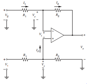
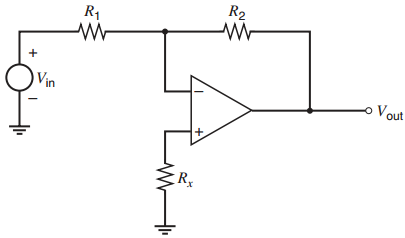
In the circuit of Fig. 6.55, determine the cor-rect value ofRxso that the output voltage is zero when the input voltage is zero. Assume a nonzero input bias current, but zero input offset current and input offset voltage.Figure 6.55 R2 R1 Vin Vout t,
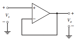
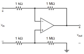
Determine the output voltage as a function of the input voltage for the circuit of Fig. 6.54. Assume the op amp is ideal.Figure 6.54 1 k2 1 ΚΩ Vout +0 Vin
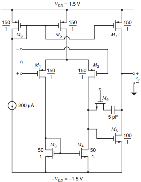
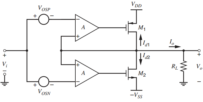
Using the schematics from Fig. 5.35 and Problem 5.24, design the output stage shown in Fig. 5.32 to satisfy the following requirements.(a) VDD = VSS = 2.5 V.(b) The standby power dissipation should be no more than 70 mW.(c) RL = 100 Ω.(d) The maximum allowed gain error with zero offsets
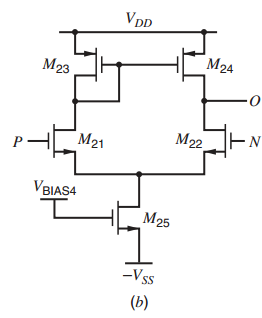
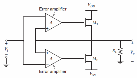
Using a circuit that is the complement of the one in Fig. 5.35, draw the schematic for the bottom error amplifier and output transistor M2, which are shown in block diagram form in Fig. 5.32. In the error amplifier, label the transistors as M21-M27, where M21is the complement of M11, M22is the
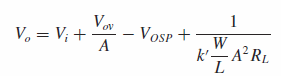
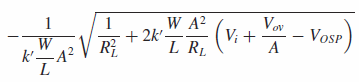
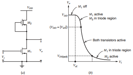
For the circuit in Fig. 5.34, assume that the input voltage Viis high enough that M1operates in the active region but M2is cut off. Using the same assumptions as in the derivation of (5.116), show that Vois related to Viby the following expressionFigure 5.34: Voy Vosp + V. = V; + k'-A² RL A W A?
Design a CMOS output stage based on the circuit of Fig. 5.31 to deliver ±1 V before clipping at Vowith RL = 1 kΩ and VDD= VSS= 2.5 V. Use 10 µA bias current in M3and 100 µA idling current in M1and M2. Set (W/L)3= 50/1 and (W/L)6= 25/1. Specify the W/L for
Find the minimum output voltage for the circuit in Fig. 5.31.Figure: 5.31: VDp BIAS Mз M4 M4 RL M2 M5 M6 +o -Vss
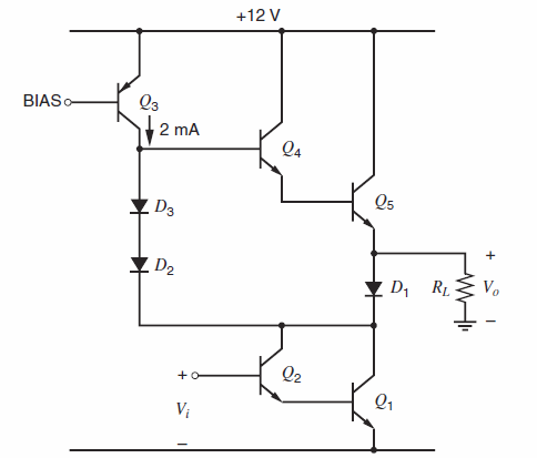
A BiCMOS Class AB output stage is shown in Fig. 5.43. Device parameters are βF(npn) = 80, βF(pnp) = 20, VBE(on)= 0.8 V, μpCox= 26 µA/V2, and Vt= ˆ’0.7 V.(a) Calculate bias currents in all devices for Vo = 0.(b) Calculate the positive and
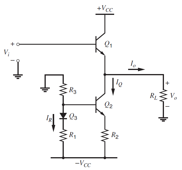
For the circuit of Fig. 5.25, assume that VCC= 15V, βF(pnp) = 30, βF(npn) = 150, IS(npn) = 10ˆ’14A, IS(pnp) = 10ˆ’15A, and for all devices VBE(on)= 0.7 V, VCE(sat)= 0.2 V. Assume that Q5and Q6are npn devices and the collector current in Q7is 0.15 mA.(a) Calculate the maximum positive
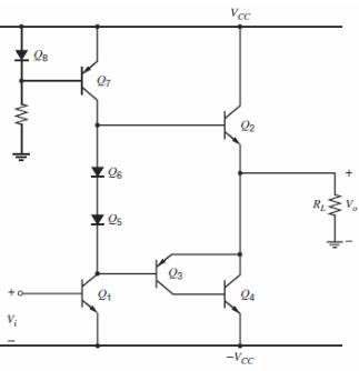
An all-npn Darlington output stage is shown in Fig. 5.42. For all devices VBE(on)= 0.7 V, VCE(sat)= 0.2 V, βF= 100. The magnitude of the collector current in Q3is 2 mA.(a) If RL = 8 Ω, calculate the maximum positive and negative limits of Vo.(b) Calculate the power
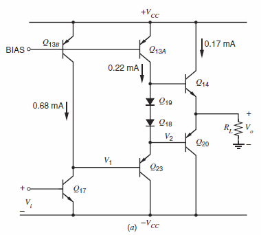
For the circuit of Problem 5.15, calculate bias currents in Q23,Q20, Q19, Q18, and Q14for Vo= ˆ’10 V with RL= 1 kΩ. Use IS= 10ˆ’14A for all devices.Data from Prob. 5.15:For the output stage of Fig. 5.20a, assume that VCC = 15 V, βF (pnp) = 50,
(a) For the circuit of Problem 5.15, calculate the maximum possible average output power than can be delivered to a load RLif the instantaneous power dissipation per device must be less than 100 mW. Also specify the corresponding value of RLand the circuit efficiency (for the output devices only).
For the output stage of Fig. 5.20a, assume that VCC= 15 V, βF(pnp) = 50, βF(npn) = 200, and for all devices VBE(on)= 0.7 V, VCE(sat)= 0.2 V, IS= 10ˆ’14A. Assume that the magnitude of the collector current in Q13Ais 0.2 mA.(a) Calculate the maximum positive and
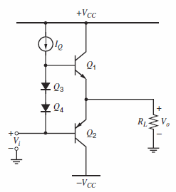
For the output stage of Fig. 5.18, assume that VCC= 15 V and for all devices VCE(sat)= 0.2 V, VBE(on)= 0.7 V, and βF= 50.Fig. 5.18:(a) Calculate the maximum positive and negative limits of Vo for RL = 10 kΩ and RL = 2 kΩ.(b) Calculate the maximum average power
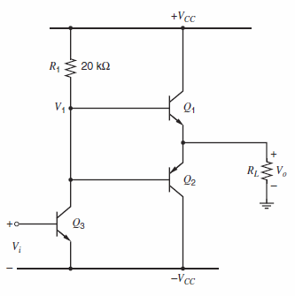
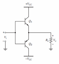
In the circuit of Fig. 5.13, VCC= 12 V, IQ= 0.1 mA, RL= 1 kΩ, and for all devices IS= 10ˆ’15A, βF= 150. Calculate the value of Viand the current in each device for Vo= 0, ± 5 V, and ± 10 V. Then sketch the transfer characteristic from Vo= 10 V to Vo=
For the circuit of Problem 5.10, calculate and sketch the waveforms of Ic1, Vce1, and Pc1for device Q1over one cycle. Do this for output voltage amplitudes (zero to peak) of 11.5 V, 6 V, and 3 V. Neglect crossover distortion and assume sinusoidal signals.Data from Prob. 5.10:The circuit of Fig.
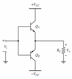
For the circuit of Fig. 5.10, assume that VCC= 12 V, RL= 1 kΩ, and VCE(sat)= 0.2 V. Assume that there is sufficient sinusoidal input voltage available at Vito drive Voto its limits of clipping. Calculate the maximum average power that can be delivered to RLbefore clipping occurs, the
The circuit of Fig. 5.10 has VCC= 15 V, RL= 2 kΩ, VBE(on)= 0.6 V, and VCE(sat)= 0.2 V.(a) Sketch the transfer characteristic from Vi to Vo assuming that the transistors turn on abruptly for Vbe = VBE(on).(b) Sketch the output voltage waveform and the collector current waveform in each
Calculate second-harmonic distortion in the common-source amplifier with a depletion load shown in Fig. 4.20a for a peak sinusoidal input voltage v̂i= 0.01 V and VDD= 3 V. Assume that the dc input voltage is adjusted so that the dc output voltage is 1 V. For simplicity, assume that the two
When the distortion is small, the second and third harmonic-distortion terms of an amplifier can be calculated from the small-signal gains at the quiescent and extreme operating points. Starting with the power series given in (5.41),(a) Calculate an expression for the small-signal gain Av =
Calculate the incremental slope of the transfer characteristic of the circuit of Fig. 5.8 at the quiescent point and at the extremes of the signal swing with vi= v̂isin ωt and v̂i= 0.5 V:a) Let A+v = Av when vi is maximum.b) Let AvQ = Av when vi = 0.c) Let
(a) For the circuit of Problem 5.1, draw load lines in the Ic - Vce plane for RL = 0 and RL→ ∞. Use an Ic scale from 0 to 30 mA. Also draw constant power hyperbolas for Pc = 0.1 W, 0.2 W, and 0.3 W. What is the maximum possible instantaneous power dissipation in Q1 for the above
Calculate the incremental slope of the transfer characteristic of the circuit of Problem 5.1 at the quiescent point and at the extremes of the signal swing with a peak sinusoidal output of 1 V and RL= 2 k„¦.Problem 5.1A circuit as shown in Fig. 5.1 has VCC = 15V, R1 = R2 = 0, R3 =
If βF= 100 for Q1in Problem 5.1, calculate the average signal power delivered to Q1by its driver stage if Vois sinusoidal with an amplitude equal to the maximum possible before clipping occurs. Repeat for RL= 10 k„¦. Thus calculate the power gain of the circuit.Problem 5.1A
(a) Prove that any load line tangent to a power hyperbola makes contact with the hyperbola at the midpoint of the load line.(b) Calculate the maximum possible instantaneous power dissipation in Q1 for the circuit of Problem 5.1 with RL = 2 kΩ and RL = 10 kΩ.(c) Calculate the
(a) For the circuit of Problem 5.1, sketch load lines in the Ic- Vceplane for RL= 2 k„¦ and RL= 10 k„¦.(b) Calculate the maximum average sinusoidal output power that can be delivered to RL (both values) before clipping occurs in (a) above. Sketch corresponding waveforms for
A circuit as shown in Fig. 5.1 has VCC= 15V, R1= R2= 0, R3= 5k„¦, RL= 2k„¦, VCE(sat)= 0.2 V, and VBE(on)= 0.7 V. All device areas are equal.(a). Sketch the transfer characteristic from Vi to Vo.(b). Repeat (a) if RL = 10 k„¦.(c). Sketch the waveform of Vo if a
Repeat Problem 4.38 but replace the bipolar transistors with MOS transistors as in Problem 4.14. Assume the worst-case W/L mismatches in the transistors are ± 5 percent and the worst-case Vtmismatches are ± 10 mV. Assume the dc output voltage to ground is VSUPˆ’ |VGS3|.
Repeat Problem 4.38, but assume that 2-kΩ resistors are placed in series with the emitters of Q3and Q4. Assume the worst-case resistor mismatch is ± 0.5 percent and the worst-case pnp βFmismatch is ± 10 percent.Data from Prob. 4.38:Determine the worst-case
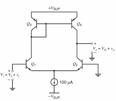
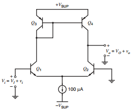
Determine the worst-case input offset voltage for the circuit of Fig. 4.58. Assume the worst-case ISmismatches in the transistors are ± 5 percent and βF= 15 for the pnp transistors. Assume the dc output voltage is VSUPˆ’ |VBE(on)|.Fig. 4.58: +VSUP Q4 Q3 V, = Vo+v, Q2 +6
A pair of bipolar current sources is to be designed to produce output currents that match with ± 1 percent. If resistors display a worst-case mismatch of ± 0.5 percent, and transistors a worst-case VBE mismatch of 2 mV, how much voltage must be dropped across the emitter resistors?
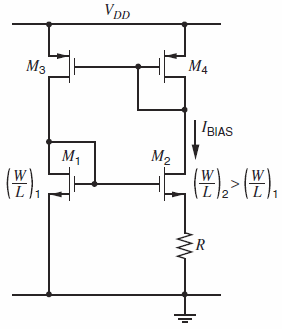
For the bias circuit shown in Fig. 4.66, determine the bias current. Assume that Xd= Ld= 0. Neglect base currents and the body effect. Comment on the temperature dependence of the bias current. Assume a channel mobility and oxide thickness from Table 2.4. Compare your calculations to a SPICE
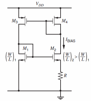
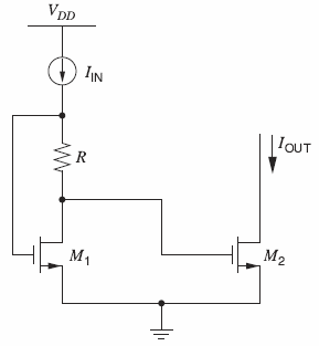
The circuit of Fig. 4.65 produces a supplyinsensitive current. Calculate the ratio of small-signal variations in IBIASto small-signal variations in VDDat low frequencies. Ignore the body effect but include finite transistor roin this calculation.Fig. 4.65: VDD M4 Мз IBIAS M1 M2 (4), (#):- (4),
Calculate the bias current of the circuit shown in Fig. 4.65 as a function of R, μnCox, (W/L)1, and (W/L)2. Comment on the temperature behavior of the bias current. For simplicity, assume that Xd= Ld= 0 and ignore the body effect. Assume M4is identical to M3.Fig. 4.65: VDD M4 M3 IBIAS
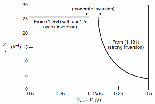
For the circuit of Fig. 4.64, find the value of W/L for which dVGS/dT = 0 at 25 °C. Assume that the threshold voltage falls 2 mV for each 1°C increase in temperature. Also, assume that the mobility temperature dependence is given by (4.243) with n = 1.5. Finally, use Table 2.4 for other
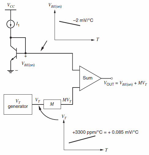
Aband-gap reference circuit is shown in Fig. 4.63. Assume that βF†’ ˆž, VA†’ˆž, IS1= 1 × 10ˆ’15A, and IS2= 8 × 10ˆ’15A. Assume the op amp is ideal except for a possibly nonzero offset voltage VOS,
Repeat Problem 4.29 assuming that the values of IS, R2, and R1are nominal but that R3is 1 percent low. Assume VBE(on)= 0.6 V.Data from Prob. 4.29:A band-gap reference like that of Fig. 4.47 is designed to have nominally zero TCF at 25°C. Due to process variations, the saturation current IS of
Simulate the band-gap reference from Problem 4.29 on SPICE. Assume that the amplifier is just a voltage-controlled voltage source with an openloop gain of 10,000 and that the resistor values are independent of temperature. Also assume that IS1= 1.25 × 10ˆ’17A and IS2= 1
A band-gap reference like that of Fig. 4.47 is designed to have nominally zero TCFat 25°C. Due to process variations, the saturation current ISof the transistors is actually twice the nominal value. Assume VOS= 0. What is dVOUT/dT at 25 °C? Neglect base currents.Fig. 4.47: Vos R2 :R3 VOUT Q2
The circuit of Fig. 4.46c is to be used as a band-gap reference. If the op amp is ideal, its differential input voltage and current are both zero andVOUT = (VBE1 + I1R1) = (VBE1 + I2R2)VOUT = VBE1 + R2 (VBE1 ˆ’ VBE2 / R3)Assume that I1 is to be made equal to 200 µA,
In the analysis of the hypothetical reference of Fig. 4.44, the current I1was assumed proportional to temperature. Assume instead that this current is derived from a diffused resistor, and thus has a TCFof ˆ’1500 ppm/ °C. Determine the new value of VOUTrequired to achieve zero TCFat
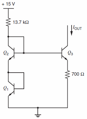
Determine the value of sensitivity S of output current to supply voltage for the circuit of Fig. 4.62, where S = (VCC/IOUT)(ˆ‚IOUT/ˆ‚VCC).Fig. 4.62: Vcc= 15 V |IOUT 10 k2 R1 Q2 1 k2 R2
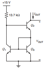
Determine the output current and output resistance of the circuit shown in Fig. 4.61.Fig. 4.61: + 15 V 13.7 k2 |'OUT Q2 700 2
Design the MOS peaking current source in Fig. 4.34 so that IOUT= 0.1 µA.(a) First, let IIN = 1 µA and find the required value of R.(b) Second, let R = 10 kΩ and find the required IIN.In both cases, assume that both transistors are identical and operate in weak inversion with
Design a MOS Widlar current source using the circuit shown in Fig. 4.31b to meet the following constraints with VDD= 3 V:(a) The input current should be 100 µA, and the output current should be 10 µA.(b) Vov1 = 0.2 V.(c) Transistor M2 must operate in the active region if the voltage
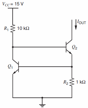
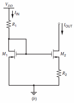
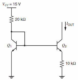
Determine the output current in the circuit of Fig. 4.60.Fig. 4.60: Vcc= 15 V 20 kΩ 1ουτ Q1 Q2 10 kΩ
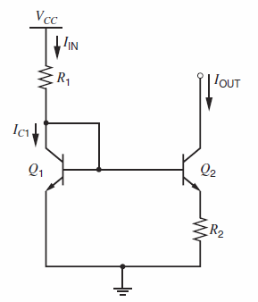
In the design of a Widlar current source of Fig. 4.31 a to produce a specified output current, two resistors must be selected. Resistor R1sets IIN, and the emitter resistor R2sets IOUT. Assuming a supply voltage of VCCand a desired output current IOUT, determine the values of the two resistors so
Design a Widlar current source using npn transistors that produces a 5 µA output current. UseFig. 4.31a with identical transistors, VCC = 30 V, and R1 = 30 kΩ. Find the output resistance.Fig. 4.31 a: Vcc IN | IOUT R1 Icı! Q2 Q1 R2
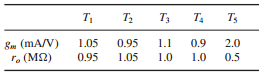
Although Gm [cm] of a differential pair with a current-mirror load can be calculated exactly from a small-signal diagram where mismatch is allowed, the calculation is complicated because the mismatch terms interact, and the results are difficult to inter-pret. In practice, the mismatch terms
Find Gm[dm] of a source-coupled pair with a current-mirror load with nonzero mismatch (Fig. 4.29b) and show that it is approximately given by (4.184). Calculate the value of Gm[dm] using the following data:Compare your answer with a SPICE simulation. Also, compare your answer to the result that
Repeat Problem 4.16 except replace the npn and pnp transistors with n-channel and p-channel MOS transistors, respectively. Assume Wn= 50[1]µm and Wp= 100[1]µm. For all transistors, assume Ldrwn= 1 µm and Xd= 0. Let ITAIL= 100 µA. Ignore the body effect. Use Table 2.3 for
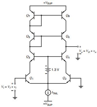
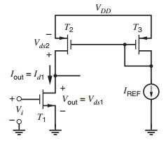
Determine the unloaded voltage gain νo/νiand output resistance for the circuit of Fig. 4.59. Neglect rμ. Verify with SPICE and also use SPICE to plot the large-signal VO-VItransfer characteristic for VSUP= 2.5V.Figure 4.59: +VSUP Os Vo+v• Q4 1.3 V Q2 V =
Repeat Problem 4.14, but now assuming that 2 k„¦ resistors are inserted in series with the sources of M3and M4. Ignore the body effect?Repeat Problem 4.14:Determine the unloaded voltage gain νo/νi and output resistance for the circuit of Fig. 4.58. Check with
Repeat Problem 4.12 except replace Q1and Q2with n-channel MOS transistors M1and M2. Also, replace Q3and Q4with p-channel MOS transistors M3and M4. Assume Wn= 50[1]m and Wp= 100 µm.Repeat Problem 4.12:Determine the unloaded voltage gain νo/νi and output resistance
Repeat Problem 4.12, but now assuming that 2-k„¦ resistors are inserted in series with the emitters of Q3and Q4.Repeat Problem 4.12:Determine the unloaded voltage gain νo/νi and output resistance for the circuit of Fig. 4.58. Check with SPICE and also use
Determine the unloaded voltage gain νo/νiand output resistance for the circuit of Fig. 4.58. Check with SPICE and also use SPICE to plot out the large-signal VO-VItransfer characteristic for VSUP= 2.5 V. Use SPICE to determine the CMRR if the current-source output
Calculate the small-signal voltage gain of a common-source amplifier with depletion load in Fig. 4.20, including both the body effect and channel-length modulation. Assume that VDD= 3 V and that the dc input voltage is adjusted so that the dc output voltage is 1 V. Assume that M1has drawn
Calculate the small-signal voltage gain of the common-source amplifier with active load in Fig. 4.16b.Assume that VDD= 3 V and that all the transistors operate in the active region. Do the calculations for values of IREFof 1 mA, 100 µA, 10 µA, and 1 µA.Figure 4.16b:(a)
Calculate the output resistance of the Wilson current mirror shown in Fig. 4.57. What is the percentage change in IOUTfor a 5-V change in VOUT? Compare your answer with a SPICE simulation using a full device model. Use SPICE to check the βFsensitivity by varying βFby −50 percent and
For the circuit of Fig. 4.56, assume that (W/L)8= (W/L). Ignoring the body effect, find (W/L)6and (W/L)7so that VDS6 = VDS7= Vov8. Draw the schematic of a double-cascode current mirror that uses the circuit of Fig. 4.56 to bias both cascade devices in the output branch. For this current
Design the circuit of Fig. 4.11b to satisfy the constraints in Problem 4.3 except the output resistance objective is that the output current change less than 0.02 percent for a 1 V change in the output voltage. Ignore the body effect for simplicity. Make all devices identical except for M4. Use
Using the data given in the example of Section 1.9, include the effects of substrate leakage in the calculation of the output resistance for the circuit of Problem 4.5. Let VOUT= 2Vand 3V?Data from 4.5Calculate the output resistance of the circuit of Fig. 4.9, assuming that IIN =100 µA and the
Calculate the output resistance of the circuit of Fig. 4.9, assuming that IIN=100 µA and the devices have drawn dimensions of 100 µm/1 µm. Use the process parameters given in Table 2.4, and assume for all devices that Xd= 0. Also, ignore the body effect for simplicity. Compare your answer
Calculate an analytical expression for the small-signal output resistance Roof the bipolar cascode current mirror of Fig. 4.8. Assume that the input current source is not ideal and that the non-ideality is modeled by placing a resistor R1in parallel with IIN. Show that for large R1, the output
Showing 200 - 300
of 376
1
2
3
4
Step by Step Answers