New Semester
Started
Get
50% OFF
Study Help!
--h --m --s
Claim Now
Question Answers
Textbooks
Find textbooks, questions and answers
Oops, something went wrong!
Change your search query and then try again
S
Books
FREE
Study Help
Expert Questions
Accounting
General Management
Mathematics
Finance
Organizational Behaviour
Law
Physics
Operating System
Management Leadership
Sociology
Programming
Marketing
Database
Computer Network
Economics
Textbooks Solutions
Accounting
Managerial Accounting
Management Leadership
Cost Accounting
Statistics
Business Law
Corporate Finance
Finance
Economics
Auditing
Tutors
Online Tutors
Find a Tutor
Hire a Tutor
Become a Tutor
AI Tutor
AI Study Planner
NEW
Sell Books
Search
Search
Sign In
Register
study help
physics
analysis and design integrated circuits
Analysis and Design of Analog Integrated Circuits 5th edition Paul R. Gray, Paul J. Hurst Stephen H. Lewis, Robert G. Meyer - Solutions
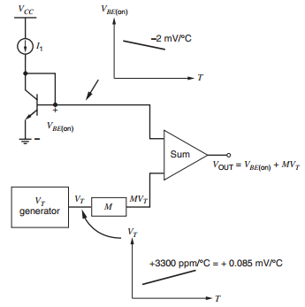
Design a simple MOS current mirror of the type show in Fig. 4.4 to meet the following constraints:Figure 4.4: Hypothetical band-gap reference circuit(a) Transistor M2 must operate in the active region for values of VOUT to within 0.2 V of ground.(b) The output current must be 50 µA.(c) The
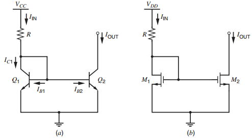
Repeat problem 4.1 including the effects of nonzero base currents?Repeat problem 4.1:Determine the output current and output resistance of the bipolar current mirror shown in Fig. 4.55. Find the output current if Vout = 1 V, 5 V, and 30 V. Ignore the effects of nonzero base currents. Compare your
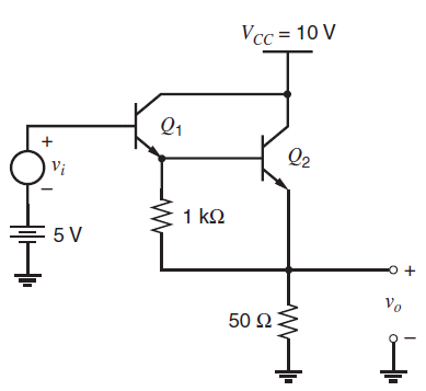
Determine the output current and output resistance of the bipolar current mirror shown in Fig. 4.55. Find the output current if Vout= 1 V, 5 V, and 30 V. Ignore the effects of nonzero base currents. Compare your answer with a SPICE simulation.Figure 4.55: Circuit for Problem 4.1Use the
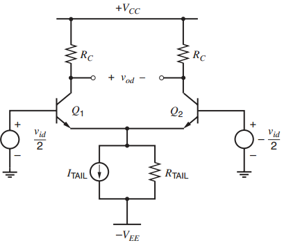
Repeat Problem 3.27 but with matched loads and mismatched transistor output resistances. Assume R1 = R2 = 10 kΩ, ro1 = 505 kΩ, and ro2 = 495 kΩ. What happens when rtail → ∞?Data from Prob. 3.27:Use half-circuit analysis to determine Adm, Acm, Acm−dm, and Adm−cm for a resistively loaded
Use half-circuit analysis to determine Adm, Acm, Acm−dm, and Adm−cm for a resistively loaded differential pair with mismatched resistive loads, R1 and R2. Assume that R1 = 10.1 kΩ and R2 = 9.9 kΩ. Also assume that gm1 = gm2 = 1 mA/V, ro1 → ∞, and ro2 → ∞. Finally, assume that the
Determine the input offset voltage of the source-coupled pair in Fig. 3.50 for which ITAIL= 50 µA. The drawn device dimensions are W = 10 µm and L = 1 µm. Use the process parameters given in Table 2.4. Assume that the worst-case W/L mismatch is 2 percent and the device thresholds
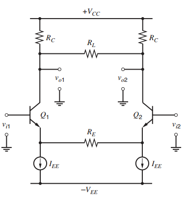
For the circuit of Fig. 3.45, determine the input offset voltage if the transistor base widths mismatch by 10 percent but otherwise the circuit is balanced. Let RTAIL†’ˆž.Fig. 3.45: +Vcc RC RC V 2 Vo1 12 Q2 Q1 Vi2 Va RTAIL ITAIL -VEE
Determine the required bias current and device sizes to design a source-coupled pair to have the following two characteristics. First, the small-signal transconductance with zero differential input voltage should be 1.0 mA/V. Second, a differential input voltage of 0.2 V should result in a
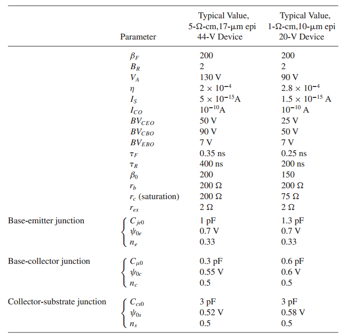
Estimate the series base resistance, series collector resistance rc, base-emitter capacitance, base-collector capacitance, and collector-substrate capacitance of the high-current npn transistor structure shown in Fig. 2.73. This structure is typical of those used as the output transistor in
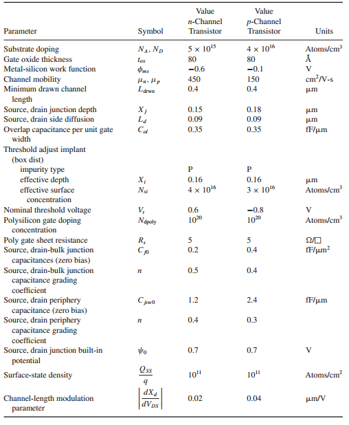
An NMOS transistor has parameters W = 10 µm, L=1 µm, k’ =194 µA/V2, λ = 0.024 V−1, tox = 80 Aͦ, ϕf = 0.3 V, Vt0 = 0.6 V, and NA = 5×10¹⁵ atoms/cm3. Ignore velocity saturation effects.(a) Sketch the ID - VDS characteristics for VDS from 0 to 3V and VGS = 0.5 V, 1.5 V, and 3 V. Assume VSB
Calculate the small-signal model parameters gm, ro, Cgs, and Cgdfor a NMOS transistor. Also calculate the gate-leakage current IG. Assume the transistor operates in the active region with ID= 100 μA, VDS= 1V, VBS= 0 V, W = 0.5 m, and L = 0.1 μm. Use the transistor model
Calculate the small-signal model parameters gm, ro, Cgs, and Cgdfor a NMOS transistor. Assume the transistor operates in the active region with ID= 100 μA, VDS= 1V, VBS= 0 V, W 0.9 μm, and L = 0.2
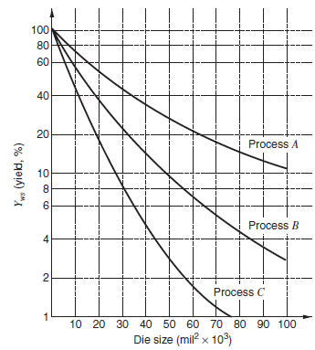
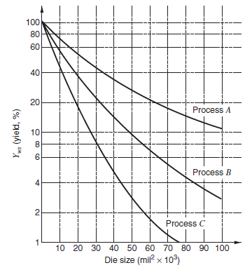
(a) A frequently used empirical approximation for the yield of an IC process as a function of die size is Yws = exp (ˆ’A/A0) where A is the die area and A0 is a constant. Using Fig. 2.68, determine approximate values of A0 for each of the three processes shown. Use the point on the curve
Determine the direct fabrication cost of an integrated circuit that is 150 mils on a side in size. Assume a wafer-fab cost of $130.00, a package and testing cost of $0.40, a die-fab yield of 0.8, and a final test yield of 0.8. Work the problem for yield curves A,B, andC in Fig. 2.68.
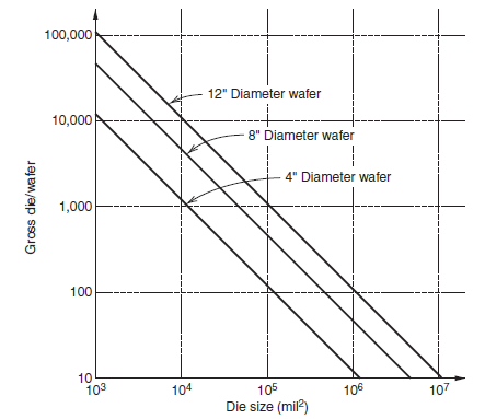
An integrated electronic subsystem is to be fabricated, which requires 40,000 square mils of silicon area. Determine whether the system should be put on one or two chips, assuming that the fabrication cost of the two chips is the only consideration. Assume that the wafer-fab cost is $100.00, the
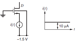
The transistor shown in Fig. 2.74 is connected in the circuit shown in Fig. 2.75. The gate is grounded, the substrate is connected to ˆ’1.5 V, and the drain is open circuited. An ideal current source is tied to the source, and this source has a value of zero for t < 0
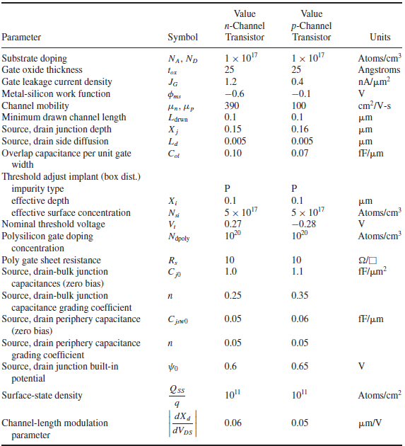
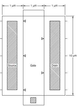
Calculate the small-signal model parameters of the device shown in Fig. 2.74, including gm, gmb, ro, Cgs, Cgd, Csb, and Cdb.Fig. 2.74 Assume the transistor is biased at a drain-source voltage of 2 V and a drain current of 20 μA. Use the process parameters that are specified in Table 2.4.
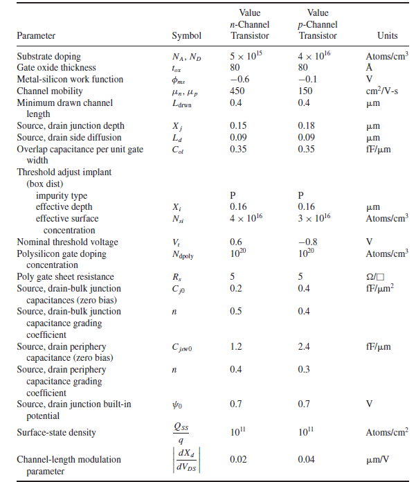
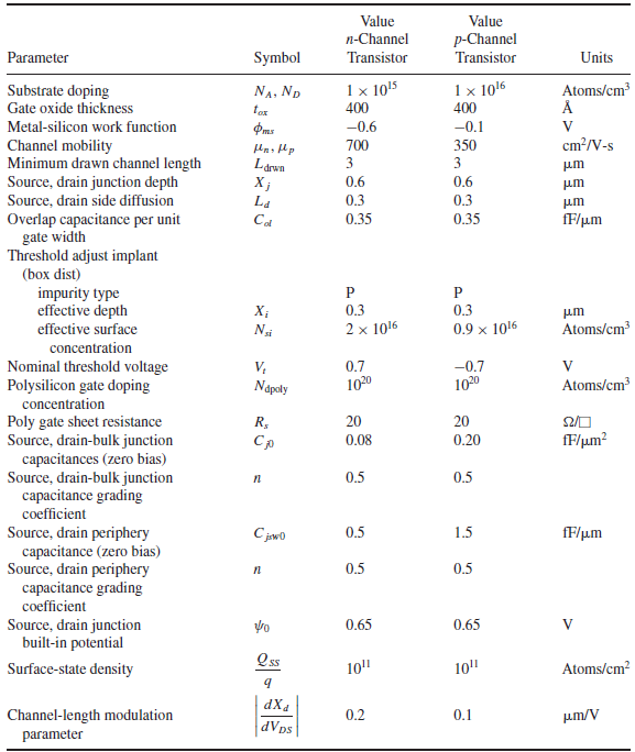
Calculate the threshold voltage of the p–channel transistors for the process given in Table 2.1.Table 2.1. First do the calculation for the unimplanted transistor, then for the case in which the device receives the channel implant specified. Note that this is a p-type implant, so that
Calculate the total parasitic junction capacitance associated with a 10-kΩ base-diffused resistor if the base sheet resistance is 100 Ω/D and the resistor width is 6 μm. Repeat for a resistor width of 12 μm. Assume the doping profiles are as shown
The substrate pnp of Fig. 2.36a is to be used as a test device to monitor epitaxial layer thickness. Assume that the flow of minority carriers across the base is vertical, and that the width of the emitter-base and collector-base depletion layers is negligible. Assume that the epi layer resistivity
If the lateral pnp structure of Fig. 2.33a is fabricated with an epi layer resistivity of 0.5 Ω-cm, determine the value of collector current at which the current gain begins to fall off. Assume a diffusivity for holes of: D̅p= 10 cm2/s. Assume a base width of 8
A base-emitter voltage of from 520 mV to 580 mV is measured on a test npn transistor structure with 10 μA collector current. The emitter dimensions on the test transistor are 100 μm × 100 μm. Determine the range of values of QB implied by this data. Use this information to calculate the range
A diffused resistor has a length of 200 μm and a width of 5 μm. The sheet resistance of the base diffusion is 100Ω/D and the emitter diffusion is 5Ω/D. The base pinched layer has a sheet resistance of 5 Ω/D. Determine the resistance of the resistor if it is an emitter-diffused, base-diffused,
Consider a hypothetical layer of silicon that has an n-type impurity concentration of 1017 cm−3 at the top surface, and in which the impurity concentration decreases exponentially with distance into the silicon. Assume that the concentration has decreased to 1/e of its surface value at a depth of
What impurity concentration corresponds to a 1 Ω-cm resistivity in p-type silicon? In n-type silicon?
Calculate the transconductance of an n-channel MOSFET at ID = 10 nA and VDS = 1 V, assuming subthreshold operation and n = 1.5. Assuming (Cgs + Cgd + Cgb) = 10 fF, calculate the corresponding device fT.
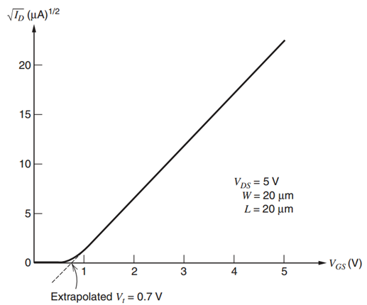
Plot ˆšIDversus VGSfor an n-channel MOSFET with W = 1 µm, L = 1 µm, k€™ = 54 µA/V2, λ = 0, VDS= 5 V, VSB= 0, Vt0= 0.7 V, and „°c= 1.5 × 10⁶V/m. Ignore sub threshold conduction. Compare the plot with Fig. 1.44a and explain
Calculate the transconductance of an n-channel MOSFET with W = 10 µm, μn = 450 cm2/(V–s), and ℰc = 1·5 × 106 V/m using channel lengths from 10 µm to 0.4 µm. Assume that tox = L / 50 and that the device operates in the active region with VGS − Vt = 0.1 V. Compare the result to a
Consider an NMOS transistor with W = 2 µm, L= 0.5 µm, k€™ =194 µA/V2, λ = 0, Vt0= 0.6V, and „°c= 1.5 × 10⁶V/m. Compare the drain current predicted by the model of Fig. 1.41 to the drain current predicted by direct calculation using
Examine the effect of velocity saturation on MOSFET characteristics by plotting ID−VDS curves for VGS = 1 V, 2 V, and 3 V, and VDS = 0 to 3 V in the following cases, and by comparing the results with and without inclusion of velocity saturation effects. Assume VSB = 0, Vt0 = 0.6 V, k’ =194
Use the device data of Problems 1.15 and 1.16 to calculate the frequency of unity current gain of this transistor with VDS = 3V, VSB = 0 V, VGS = 1 V, 1.5 V, and 2 V.Data from Prob. 1.16:Derive and sketch the complete small-signal equivalent circuit for the device of Problem 1.15 with VGS = 1 V,
Derive and sketch the complete small-signal equivalent circuit for the device of Problem 1.15 with VGS = 1 V, VDS = 2 V, and VSB = 1 V. Use ψ0 = 0.7 V, Csb0 = Cdb0 = 20 fF, and Cgb = 5 fF. Overlap capacitance from gate to source and gate to drain is 2fF.Data from Prob. 1.15:An NMOS
Sketch the graph of small-signal, common emitter current gain versus frequency on log scales from 0.1 MHz to 1000 MHz for the examples of Problems 1.8 and 1.9. Calculate the fT of the device in each case.Data from Prob. 1.9:Repeat Problem 1.8 for IC = 1 mA, VCB = 1V, and VCS = 2 V.Data
A lateral pnp transistor has an effective base width of 10 µm (1 µm = 10−4 cm).(a) If the emitter-base depletion capacitance is 2 pF in the forward-bias region and is constant, calculate the device fT at IC = −0.5 mA. (Neglect Cμ.) Also, calculate the minority-carrier
An integrated npn transistor has the following characteristics: τF= 0.25 ns, small-signal, short-circuit current gain is 9 with IC =1 mA at f = 50 MHz, VA = 40 V, β0 = 100, rb = 150Ω, rc = 150Ω, Cμ = 0.6 pF, Ccs
Consider the circuit of Fig. 3.80 except replace both npn transistors with n-channel MOS transistors. Neglect the body effect, and assume λ = 0. Use half-circuit concepts to determine the differential-mode and common-mode gain of this modified circuit.Fig. 3.80: +Vcc Rc Rc RL Vo2 Vo1
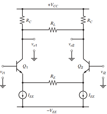
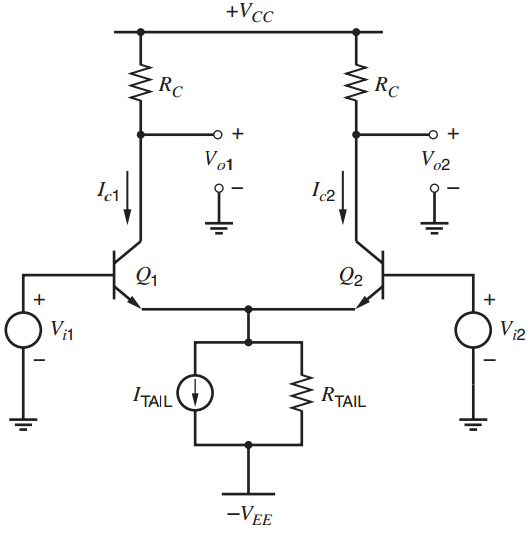
Use half-circuit concepts to determine the differential-mode and common-mode gain of the circuit shown in Fig. 3.80. Neglect ro, rμ, and rb. Calculate the differential-mode and common-mode input resistance.Fig 3.80: +Vcc RC RC RL Vo2 Vo1 Q2 Vi2 Q1 RE Vi1 IEE IEE LEE -V EE
Determine the overall input resistance, voltage gain, and output resistance of the CC-CB connection of Fig. 3.79. Neglect ro, rμ, and rb. Note that the addition of a 10-kΩ resistor in the collector of Q1would not change the results, so that the results of the
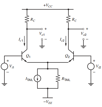
Repeat Problem 3.18, but with the addition of emitter-degeneration resistors of value 4 kΩ each.Data from Prob. 3.18:Determine the differential-mode gain, common-mode gain, differential-mode input resistance, and common-mode input resistance for the circuit of Fig. 3.45 with ITAIL = 20
Determine the differential-mode gain, common-mode gain, differential-mode input resistance, and common-mode input resistance for the circuit of Fig. 3.45 with ITAIL= 20 µA, RTAIL= 10 MΩ, RC = 100 kΩ, and VEE = VCC = 5 V. Neglect rb, ro, and rμ.
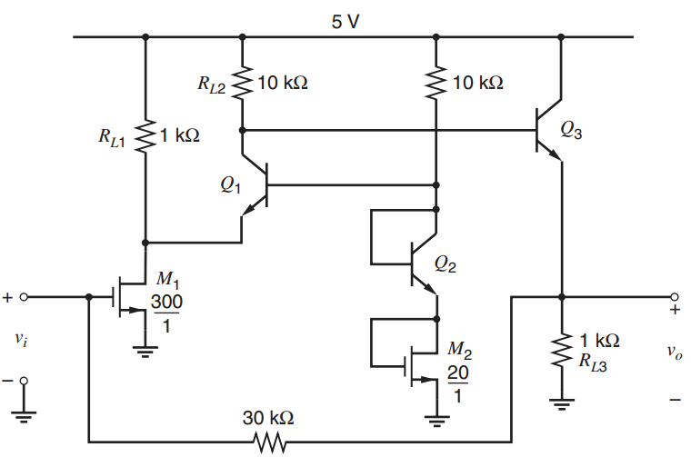
A BiCMOS amplifier is shown in Fig. 3.78. Calculate the small-signal voltage gain vo / vi. Assume IS= 10ˆ’16A, βF= 100, rb= 0, VA†’ ˆž, μnCox= 200 µA / V2, Vt= 0.6 V, and λ= 0. Check your answer with SPICE and then use
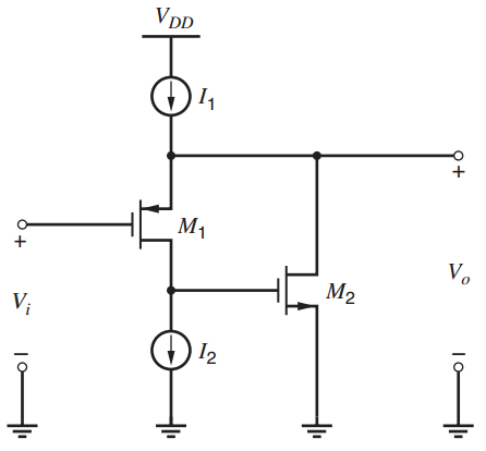
Find the short-circuit transconductance of the super-source follower shown in Fig. 3.43. Assume I1 = 200 µA, I2 = 100 µA, W1= 30 µm, and W2= 10 µm. Also, assume that both transistors operate in the active region, and ignore the body effect. Use the transistor parameters in
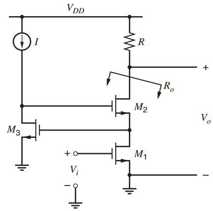
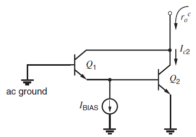
Find the output resistance for the active-cascode circuit of Fig. 3.77 excluding resistor R. Assume that all the transistors operate in the active region with dc drain currents of 100 µA. Use the transistor parameters in Table 2.4. Ignore the body effect. Assume W = 10µm, Ldrwn= 0.4µm, and
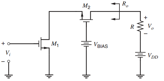
Determine the input resistance, transconductance, output resistance, and maximum open-circuit voltage gain for the CS-CG circuit of Fig.3.38 if ID1 = ID2= 250 µA. Assume W/L=100, λ=0.1 V−1, and χ = 0.1. Use Table 2.2 for other parameters.Fig. 3.38:Table 2.2: Ro M2 V. V BIAS VDD
Determine the input resistance, transconduc-tance, output resistance, and maximum open-circuit voltage gain for the CE-CB circuit of Fig. 3.36 if IC1 = IC2 = 250 µA.Fig. 3.36: R. Q2 VBIAS VpD V,
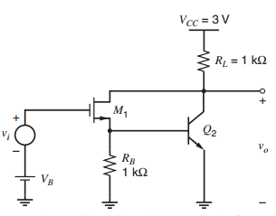
A BiCMOS Darlington is shown in Fig. 3.76. The bias voltage VBis adjusted for a dc output voltage of 2 V. Calculate the bias currents in both devices and then calculate the small-signal voltage gain Ï…o/Ï…iof the circuit. For the MOS transistor, assume W = 10µm,
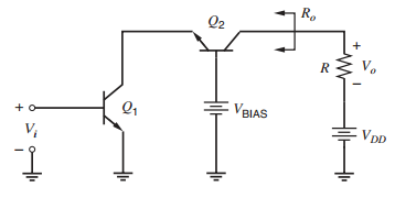
Calculate the output resistance rcoof the common-emitter Darlington transistor of Fig. 3.75 as a function of IBIAS. Do not neglect either ro1or ro2in this calculation, but you may neglect rband rμ. If IC2= 1mA, what is rcofor IBIAS= 1mA? For IBIAS= 0?Figure 3.75 12 Q2 ac ground IBIAS
Determine the dc collector currents in Q1and Q2, and then the input resistance and voltage gain for the Darlington emitter follower of Fig. 3.74. Neglect rμ, rb, and ro. Assume that VBE(on)= 0.7V. Check your answer with SPICE and also use SPICE to determine the output resistance of
For the common-drain amplifier of Fig. 3.73, assume W/L = 10 and λ = 0. Use Table 2.2 for other parameters. Find the dc output voltage VOand the small-signal gain νo/νiunder the following conditions:(a) Ignoring the body effect and with R †’
Determine the input resistance, voltage gain ν0/ ν s, and output resistance of the CC amplifier of Fig. 3.23 a if RS= 5k „¦, RL= 500 „¦, and IC= 1mA. Neglect rband ro. Do not include RSin calculating the input resistance. In calculating the
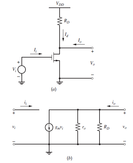
Determine the input resistance of the CG amplifier of Fig. 3.19 if the transistor operates in the active region with ID = 100 μA. Let RD= 10 k „¦, μnCox= 200 μA/V2, λ = 0.01Vˆ’1, W = 100 μm, and L = 1
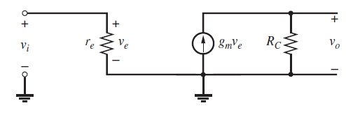
Assume that RCis made large compared with roin the CB amplifier of Fig. 3.15. Use the equivalent circuit of Fig. 3.17 and add robetween the input (emitter terminal) and the output (collector terminal) to calculate the output resistance when(a) The amplifier is driven by an ideal current source.(b)
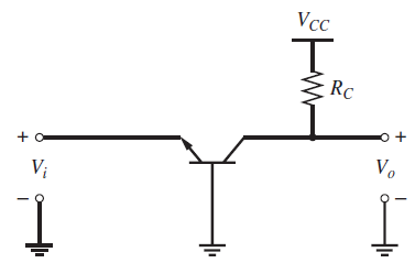
Determine the input resistance, transconductance, and output resistance of the CB amplifier of Fig. 3.15 if IC= 250μA and RC= 10 k „¦. Neglect rband ro.Figure 3.15 Vcc Rc Vo V;
For the common-source amplifier of Fig. 3.12, calculate the small-signal voltage gain and the bias values of Viand Voat the edge of the triode region. Also calculate the bias values of Viand Vowhere the small-signal voltage gain is unity with the transistor operating in the active region. What is
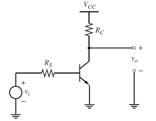
Assume that RS= RC= 50k „¦ in Problem 3.2, and calculate the optimum IC. What is the dc voltage drop across RC? What is the voltage gain?In problem 3.2A CE transistor is to be used in the amplifier of Fig. 3.72 with a source resistance RS and collector resistor RC. First, find the
A CE transistor is to be used in the amplifier of Fig. 3.72 with a source resistance RSand collector resistor RC. First, find the overall small-signal gain vo/vias a function of RS, RC, β0, VA, and the collector current IC. Next, determine the value of dc collector bias current ICthat
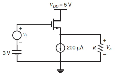
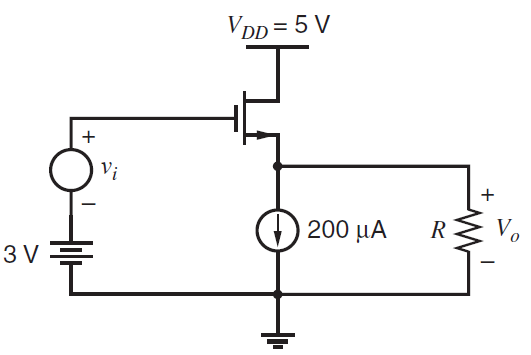
Determine the input resistance, transconductance, and output resistance of the CE amplifier of Fig. 3.7 if RC= 20 k and IC= 250μ A. Assume that rb= 0.Figure 3.7 VDD = 5 V V; Vo 200 μΑ R
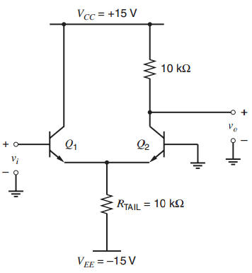
Design an emitter-coupled pair of the type shown in Fig. 3.53a. Assume ITAIL= 0 and select values of RCand RTAILto give a differential input resistance of 2 MΩ, a differential voltage gain of 500, and a CMRR of 500. What are the minimum values of VCCand VEEthat will yield this
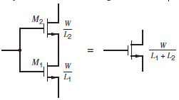
Show that two MOS transistors connected in series with channel lengths of L1and L2and identical channel widths of W can be modeled as one equivalent MOS transistor whose width is W and whose length is L1+ L2, as shown in Fig. 2.77.Assume the transistors are identical except
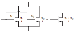
Show that two MOS transistors connected in parallel with channel widths of W1and W2and identical channel lengths of L can be modeled as one equivalent MOS transistor whose width is W1+ W2and whose length is L, as shown in Fig. 2.76. Assume the transistors are
An n-channel implanted transistor from the process described in Table 2.1 displays a measured output resistance of 5 MΩ at a drain current of 10 μA, biased in the active region at a VDSof 5 V. Table 2.1The drawn dimensions of the device are 100 μm by 7
An MOS transistor biased in the active region displays a drain current of 100 μA at a VGS of 1.5 V and a drain current of 10 μA at a VGS of 0.8 V. Determine the threshold voltage and μn Cox (W/L). Neglect subthreshold conduction and assume that the mobility is constant.
A base-emitter voltage of 480 mV is measured on a super-β test transistor with a 100 μm × 100 μm emitter area at a collector current of 10 μA. Calculate the QB and the sheet resistance of the base region. Estimate the punch-through voltage in the following way. When the base depletion region
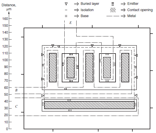
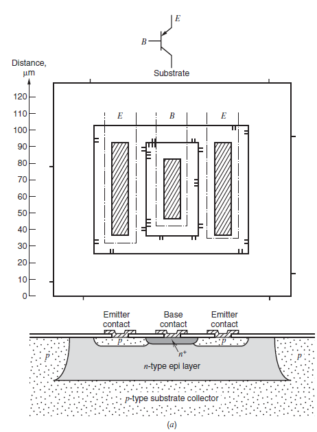
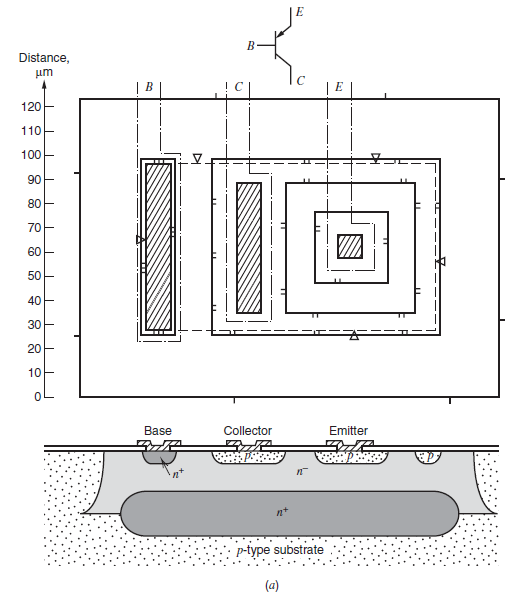
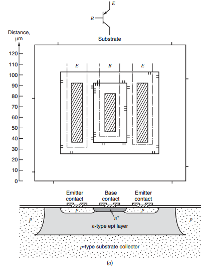
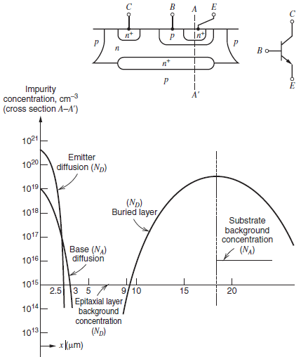
For the substrate pnp structure shown in Fig. 2.36 a, calculate IS,Cje,Cμ, andÏ„F.Assume the doping profiles are as shown in Fig. 2.17.Figure 2.36 (a)Figure 2.17 Distance, Substrate um 120- 110- 100- 50 10 Emitter Base Emitter contact contact contact п-type epi layer p-type
What is the sheet resistance of a layer of 1 Ω-cm material that is 5 mm thick?
An integrated-circuit npn transistor has the following measured characteristics: rb = 100Ω, rc = 100Ω, β0 = 100, ro = 50 kΩ at IC =1 mA, fT = 600 MHz with IC = 1 mA and VCB = 10 V, fT = 1 GHz with IC = 10 mA and VCB = 10 V,
Repeat Problem 1.8 for IC = 1 mA, VCB = 1 V, and VCS = 2 V.Data from Prob. 1.8:Derive and sketch the complete small-signal equivalent circuit for a bipolar transistor at IC = 0.2 mA, VCB = 3V, VCS = 4 V. Device parameters are Cje0 = 20 fF, Cμ0 = 10 fF, Ccs0 = 20 fF, β0 =
If junction curvature causes the maximum field at a practical junction to be 1.5 times the theoretical value, calculate the doping density required to give a breakdown voltage of 150 V with an abrupt pn junction in silicon. Assume that one side of the junction is much more heavily doped than the
Calculate the zero-bias junction capacitance for the example in Problem 1.1, and also calculate the value at 5 V reverse bias and 0.3 V forward bias. Assume a junction area of 2 × 10⁻⁵ cm2.Data from Prob. 1.1Calculate the built-in potential, depletion-layer depths, and maximum field in a
(a) Calculate the built-in potential, depletion layer depths, and maximum field in a plane-abrupt pn junction in silicon with doping densities NA = 8 × 10¹⁵ atoms/cm3 and ND = 1017 atoms/cm3. Assume a reverse bias of 5 V.(b) Repeat (a) for zero external bias and 0.3 V forward bias.
Derive and sketch the complete small-signal equivalent circuit for a bipolar transistor at IC = 0.2 mA, VCB = 3V, VCS = 4 V. Device parameters are Cje0 = 20 fF, Cμ0 = 10 fF, Ccs0 = 20 fF, β0 = 100, τF= 15 ps, η = 10−3, rb = 200 Ω, rc = 100 Ω,
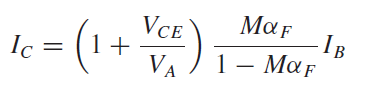
(a) Sketch theIC -VCE characteristics in the forward-active region for an npn transistor with βF = 100 (measured at low VCE), VA = 50 V, BVCBO = 120 V, and n = 4. UseWhere M is given by (1.78).
Calculate the breakdown voltage for the junction of Problem 1.1 if the critical field is ℰcrit = 4 × 10⁵ V/cm.Data from Prob. 1.1Calculate the built-in potential, depletion-layer depths, and maximum field in a plane-abrupt pn junction in silicon with doping densities NA = 8 × 10¹⁵
Repeat Problem 1.5 for a doping density of 1015 atoms/cm3 and βF = 400.Data from Problem 1.5:If the collector doping density in a transistor is 6 × 10¹⁵ atoms/cm3, and is much less than the base doping, find BVCEO for βF = 200 and n = 4. Use εcrit = 3 × 10⁵ V/cm.
If the collector doping density in a transistor is 6 × 10¹⁵ atoms/cm3, and is much less than the base doping, find BVCEO for βF = 200 and n = 4. Use ℰcrit = 3 × 10⁵ V/cm.
If the area of the transistor in Problem 1.11 is effectively doubled by connecting two transistors in parallel, which model parameters in the small-signal equivalent circuit of the composite transistor would differ from those of the original device if the total collector current is unchanged? What
Showing 300 - 400
of 376
1
2
3
4
Step by Step Answers