New Semester
Started
Get
50% OFF
Study Help!
--h --m --s
Claim Now
Question Answers
Textbooks
Find textbooks, questions and answers
Oops, something went wrong!
Change your search query and then try again
S
Books
FREE
Study Help
Expert Questions
Accounting
General Management
Mathematics
Finance
Organizational Behaviour
Law
Physics
Operating System
Management Leadership
Sociology
Programming
Marketing
Database
Computer Network
Economics
Textbooks Solutions
Accounting
Managerial Accounting
Management Leadership
Cost Accounting
Statistics
Business Law
Corporate Finance
Finance
Economics
Auditing
Tutors
Online Tutors
Find a Tutor
Hire a Tutor
Become a Tutor
AI Tutor
AI Study Planner
NEW
Sell Books
Search
Search
Sign In
Register
study help
physics
analysis and design integrated circuits
Analysis and Design of Analog Integrated Circuits 5th edition Paul R. Gray, Paul J. Hurst Stephen H. Lewis, Robert G. Meyer - Solutions
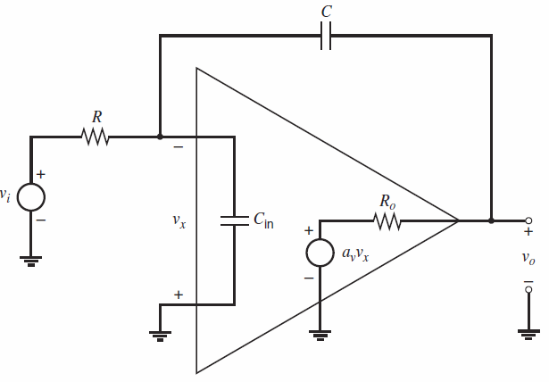
For the op amp in Fig. 12.2, use the device data and operating point from the first example in Section 12.4.1. Assume all transistors operate in the active region. (a) Find the element values in the two models for the output ports in Fig. 12.7.(b) Find the element values in the two models for
For the op amp in Fig. 12.2, use the data from Problem 12.4 except use ID5= 100 µA and |Vov| = 0.1 V for all transistors. Assume all transistors operate in the active region with Cgs= 180 fF And Cgd= 20 fF.(a) Find the element values in the two models for the output ports in Fig. 12.7.(b)
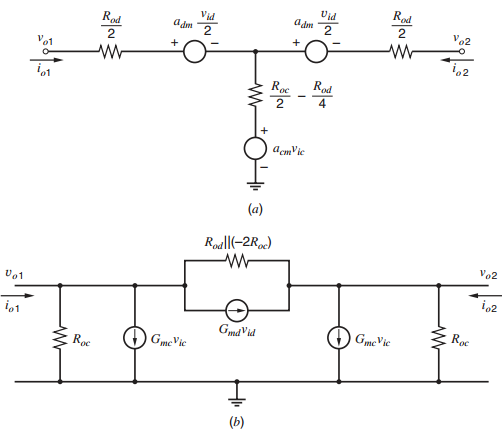
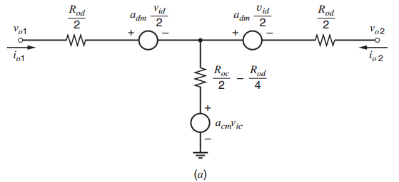
(a) For the op amp in Problem 12.5, calculate a€™cm. Assume that the CMFB scheme in Fig. 12.17 is used and that acms= 1. Recall that a€™cm= voc/vicwhen the CMFB loop is active.(b) Use SPICE to plot |a€™cm| from 100 Hz to 100 MHz.Fig. 12.17:Data from Prob. 12.5:Use the
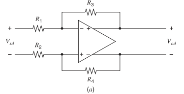
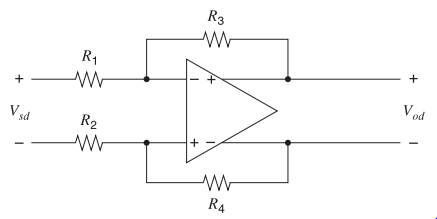
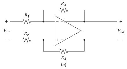
The op amp in Problem 12.5 is connected in feedback as shown in Fig. 12.32 a. The CMFB is as described in Problem 12.6. Compute the low-frequency closed-loop gains Adm= vod/vsdand Acm = voc/vscif R1 = R2= R3= R4= 100 MΩ.Figure 12.32 (a): R3 R1 V od Vad R2 R4 (a)
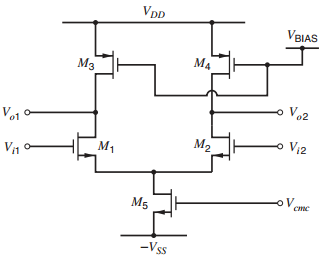
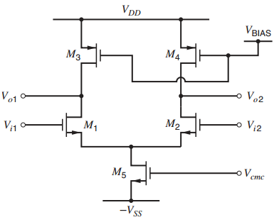
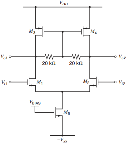
Calculate the DM output slew rate dVod/dt for the op amp in Fig. 12.2. Assume ID5= 200 µA and a 5 - pF capacitor is connected from each op-amp output to ground.Fig. 12.2: Vpp VBIAS M4 Мз Vo2 Vo1 Vi2 M2 M1 Vi1 V eme Ло сте M5 -Vss
Calculate the CM output slew rate dVoc / dt for the op amp in Fig. 12.2. Assume ID5= 200 µA and a 5€“pF capacitor is connected from each op-amp output to ground.Figure 12.2: Vpp VBIAS M4 Мз Vo2 Vo1 Vi2 M2 M1 Vi1 V eme Ло сте M5 -Vss
Compute the output slew rate dVod / dt for the op amp in the example in Section 12.6.1. Use the bias currents from the example and C = 1.39 pF.
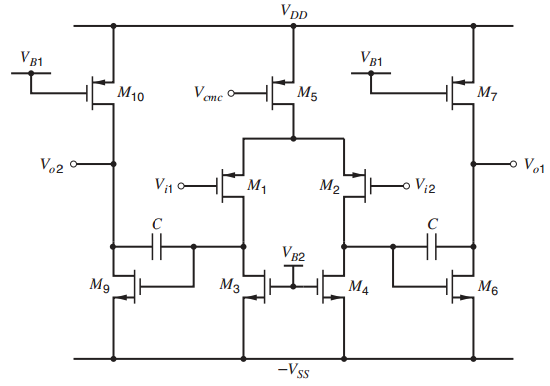
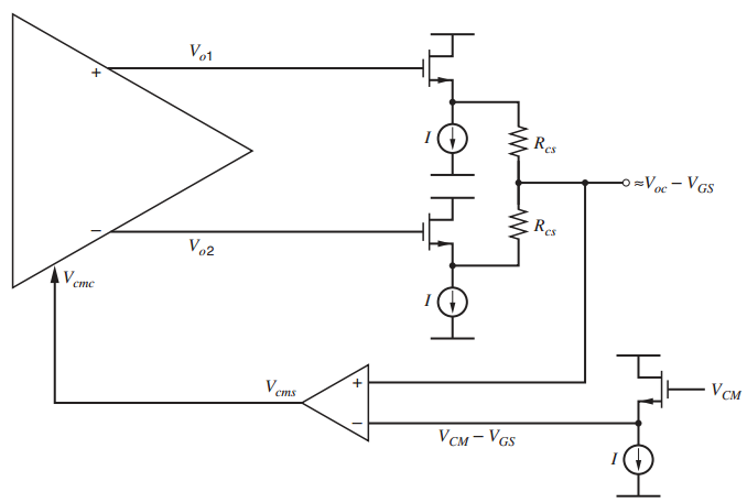
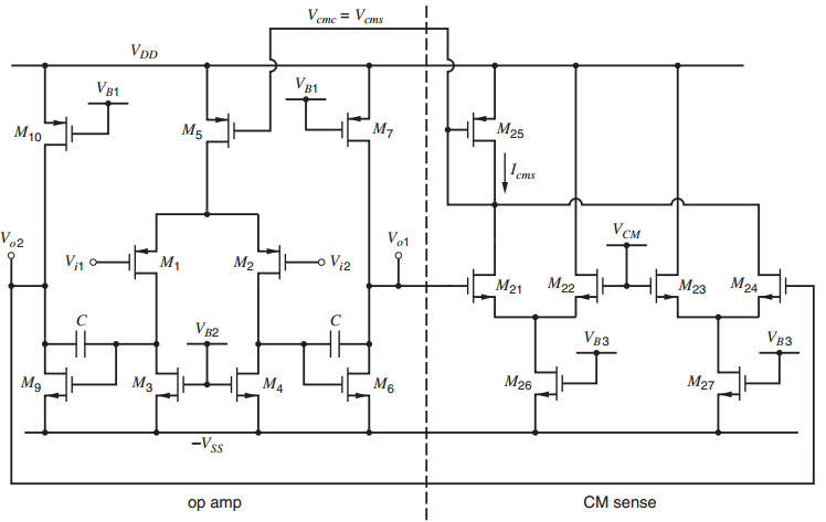
For this problem, use the op amp in Fig. 12.23 and the CMFB scheme in Fig. 12.17. Use the complement of the amplifier in Fig. 12.16b as the CM-sense amplifier, modified to give a negative dc gain. Assume the source followers in Fig. 12.17 have a low-frequency gain of 0.95 and Rcs= 15
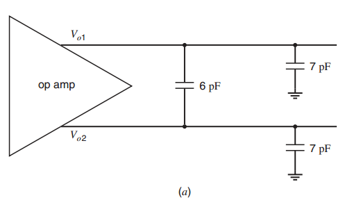
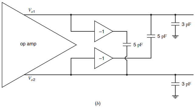
Compute the op-amp CM and DM load capacitances for the output loading in Fig. 12.53 a and 12.53 b. Assume the inverting voltage buffers in Fig. 12.53 b are ideal.Figure 12.53 (a):Figure 1253 (b): Vo1 7 pF 6 pF op amp Vo2 7 pF (a) Vo1 3 pF -1 5 pF 5 pF op amp -1 Vo2 3 pF (b)
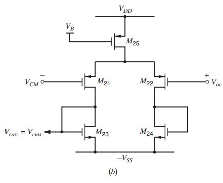
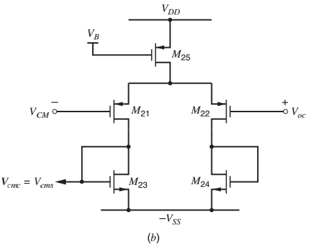
(a) For the amplifier in Fig. 12.16 b, estimate the pole associated with the RC time constant at the Vcmsoutput node. Assume |ID25| = 0.4 mA, Vov23= 0.2 V, and VOC= VCM. Ignore all capacitances except Cgs23 in parallel with a fixed capacitance of 90 fF. Take Leff= 0.80 µm. Use the data in
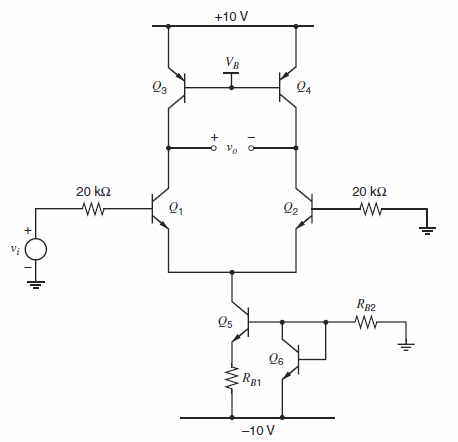
A differential amplifier with local CMFB is shown in Fig. 12.54. Use |Vov| = 0.2 V for all transistors, Vtn= ˆ’Vtp= 0.6 V, ID5= 200 µA, VAn= 10 V, |VAp| = 20 V, and γ = 0. Assume VDD= VSS= 2.5V and Vic= 0.(a) What is the dc common-mode output voltage of this
A differential amplifier that does not use a tail current source is shown in Fig. 12.55.(a) Compute the low-frequency gains adm and acm. For all transistors, drain currents are 100 µA and |Vov| = 0.2 V. Also, VAn = 10 V, and |VAp| = 20 V.(b) Compare these gains with the gains calculated in
(a) For the op amp in Fig. 12.2, assume the CM and DM load capacitances are CLc= CLd= 2 pF. Calculate the frequencies at which |adm(jω) | = 1 and |acmc(jω) | = 1, ignoring other capacitors. Use |Vov| = 0.25 V for all transistors, Vtn= ˆ’Vtp= 0.6 V, ID5= 200
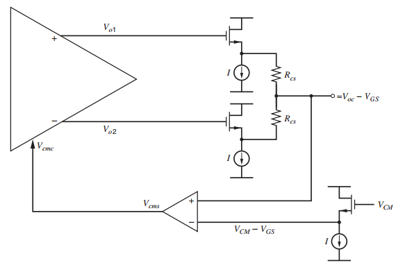
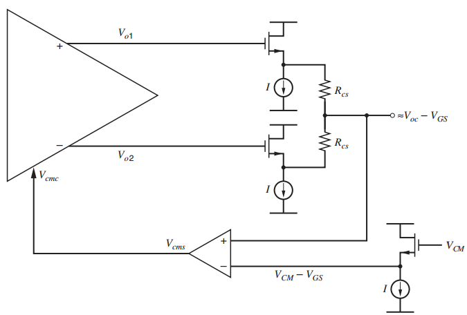
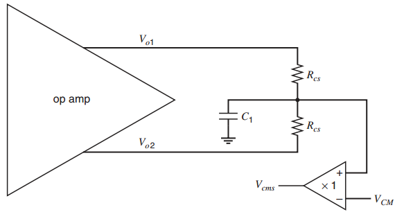
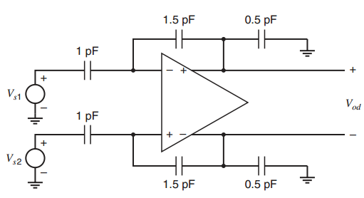
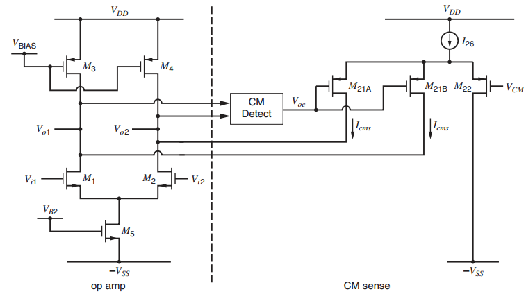
For the CM-detector in Fig. 12.56, find acms(s) = vcms(s) / voc(s), assuming the CM-sense amplifier is ideal with unity gain. Then find acms(s) when a capacitor Ccsis connected in parallel with each resistor Rcs. What is the effect of the Ccscapacitors?Figure 12.56: Vo1 Res op amp C1 Res Vo2 V cms
A NMOS transistor is operating in the triode region. Find a formula for its transconductance gm = ∂Id / ∂Vgs. Compare it with gm in the active region at the same dc drain current. Which is larger?
For the fully differential circuit in Fig. 12.32 a, assume the op amp is ideal with Ri= ˆž, Ro= 0, adm= ˆ’ ˆž, and acm= 0. Find the closed-loop gains Adm= vod/vsd, Acm= voc/vsc, Admˆ’cm= voc / vsd, and Acmˆ’dm= vod/ vsc, under the following
For the circuit in Problem 12.20 a, the applied source voltage is a single-ended signal with Vs1 = 0.2 V sin (100t) and Vs2 = 0. Assume a CMFB loop forces VOC = 0. What are Vo1 (t), Vo2 (t), Vod (t), and Voc (t)? What are Vi1 (t), Vi2 (t), Vid (t), and Vic (t)?Data from Problem 12.20:(a)
The op amp in Problem 12.4 is used with the CMFB scheme shown in Fig. 12.17. The circuit is perfectly balanced except that the CM-sense resistors are mismatched with the upper resistor Rcs1= 10.1 kΩ and the lower resistor Rcs2= 9.9 kΩ. Assume the source followers and the
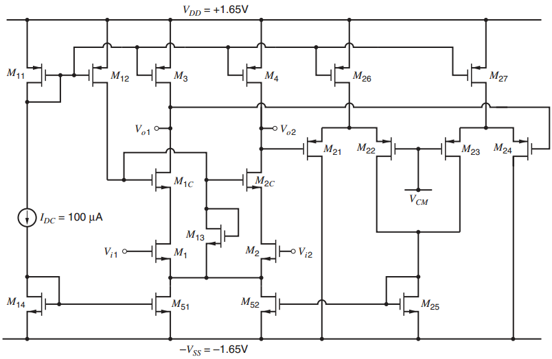
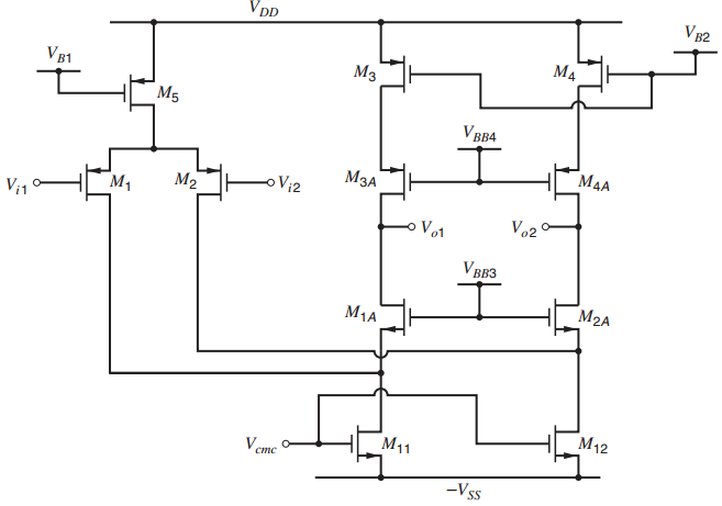
A fully differential op amp with CMFB is shown in Fig. 12.57. For M1, M1C, M2, and M2C, use W/L = (64 µm) / (0.8 µm). For M3 €“ M4, M26 €“ M27and M11, W / L = (96 µm) / (1.4 µm). For M21€“ M24, W / L = (6 µm) / (0.8 µm).
The feedback circuit in Fig. 12.58 is a switched-capacitor circuit during one clock phase. Assume the op amp is the folded-cascode op amp in Fig. 12.31.(a) Calculate the DM and CM output load capacitances, considering only the capacitances in the Fig. 12.58.(b) If the op-amp bias currents are |ID3|
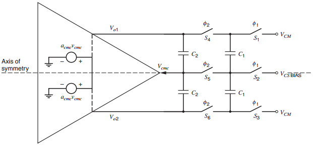
In the switched-capacitor CMFB scheme in Fig. 12.21, C1= 0.1 pF and C2= 0.5 pF.(a) With VCSBIAS = ˆ’1 V, VOC = VCM = 0.5 V. If VCSBIAS changes to ˆ’1.1 V, what is the new value of VOC? Assume |acmc| >> 1.(b) Ignoring all capacitors except C1 and C2, what are the CM and DM
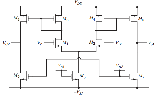
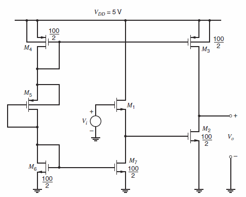
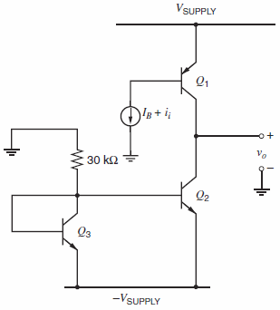
A current-mirror op amp is shown in Fig. 12.59. Assume all NMOS transistors are matched and all PMOS transistors are matched. Use |Vov| = 0.2 V for all transistors, Vtn= ˆ’Vtp= 0.6 V, ID5= 200 µA, VAn= 10 V, |VAp| = 20 V, and γ = 0. Assume VDD= VSS= 1.65 V and Vic= 0.(a)
Find the low-frequency value of a’cm for the two-stage op amp in the example in Section 12.6.1. Use the data in that example. Recall that a’cm = voc/vic when the CMFB loop is active.
Assume that the CMFB circuit in the example in Section 12.6.1 is changed so that the CM-sense amplifier has a low-frequency gain |acms0| = 2.5. Determine the compensation capacitor C needed in the op amp to assure that the CMC and DM feedback loops in the example have a phase margin of 45◦ or
Neutralization capacitors Cn are to be added to cancel the Miller effect on Cgd1 and Cgd2 in the two-stage op amp in the example in Section 12.6.1.(a) Show how the Cn capacitors should be connected in the op amp. What value of Cn should be used?(b) If these capacitors are constructed from MOS
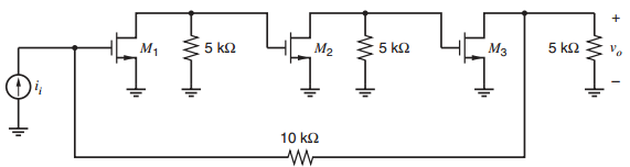
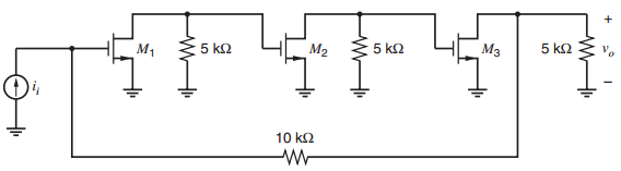
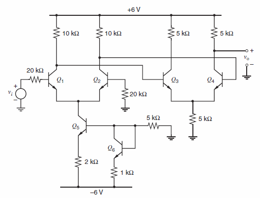
Modify the CMFB schematic in Fig. 12.26 to inject currents at the drains of M1and M2, in a manner similar to that shown in Fig. 12.18. Give a set of bias current values on the schematic. Assume ID3 = ID4= 150 µA and ID6= ID9= 400 µA.Fig. 12.26:Fig. 12.18 Veme = Vems сте VDD VB1
A fully differential op amp with mismatch is connected in the feedback circuit in Fig. 12.32a With R1= R2=10 kΩ and R3= R4= 40 kΩ. The op amp model is shown in Fig. 12.37 where adm= ˆ’181, acm= ˆ’2.89, acmc= ˆ’226, adm ˆ’ cm= 8.95,
For the op amp in Fig. 12.40, what is the common-mode input range (CMIR) if only M1and M2are changed to low-threshold devices with threshold voltages Vt1= Vt2= 0.3V?Fig. 12.40: VDD M12 M11 BiasB Мал M1A BiasC M2 M1 MAA Мзл BiasD BiasA M4 Мз CMC M5 M6
For the op amp in Fig. 12.40, what are the output voltage swing limits of Vo1 and Vo2if the thresh-old voltages of only M1A, M2A, M3A, and M4Aare changed toVt1A= Vt2A= ˆ’0.3 V and Vt3A= Vt4A= 0.3V?Figure 12.40: VpD M12 M11 BiasB M2A M1A BiasC Vo2 Vo1 M2 V1 M1 M4A Мзл BiasD BiasA
For the feedback circuit in Fig. 12.46, the capacitor values are C1 = C2 = 4 pF and CL = 6 pF. The op amp is the folded-cascode amplifier in Fig. 12.40 with low-frequency gainadm0= 1280 and gm1= 30 mA/V.(a) What is the low-frequency value of the differential-mode return ratio?(b)
For the feedback circuit in Fig. 12.46 using the op amp in Fig. 12.40, the capacitor values are C1= C2= 4 pF and CL = 6 pF. What is the differential-mode output slew rate?Fig. 12.46:Fig. 12.40: BiasE BiasE Ф2 C2 CL Vo1 01 V,1 CMC V od 92 o VBB Ф2 V sd Ф1 V02 C1 C1 V32 42 C2 $2 BiasE BiasE
For the feedback circuit in Fig. 12.46, C1= C2= 4 pF. The op amp is the folded-cascode amplifier in Fig. 12.40 with low-frequency gain adm0 = 1280 and gm1= 30 mA/V. What value of CLwill give ωτ= 1.0 Grad/s for the unity-gain frequency of the differential-mode return
If W/Lis doubled for M1= M2(i.e., m1= m2= 20), what is the new low-frequency DM op-amp gain adm0for the op amp in Fig. 12.40? Assume the bias conditions and operating regions do not change.Fig. 12.40: VpD M12 M11 BiasB M2A M1A BiasC Vo2 Vo1 M2 V1 M1 M4A Мзл BiasD BiasA M4 Мз CMC M5 M6
Calculate the spectrum of the input-referred 1/f voltage noise for the op amp in Fig. 12.40.Use (11.69) with Kf = 4.8 × 10ˆ’25 V2 €“F for NMOS devices and Kf = 8.3 × 10ˆ’26 V2 €“F for PMOS devices. Use Cox = 6.9 ×
Calculate the spectrum of the input-referred thermal noise voltage for the op amp in Fig. 12.40 if W/L is doubled for M1= M2(i.e., m1= m2= 20). Assume the bias conditions and operating regions are not changed.Fig. 12.40: VpD M12 M11 BiasB M2A M1A BiasC Vo2 Vo1 M2 V1 M1 M4A Мзл BiasD BiasA M4
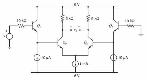
A BiCMOS Darlington is shown in Fig. 11.51. Neglecting frequency effects, calculate the equivalent input noise voltage and current generators for this circuit, assuming that the dc value of Viis adjusted for IC1= 1 mA. Device data is μn Cox= 60 µA/V2, Vt= 0.7 V,
Repeat Problem 9.9 if the circuit is compensated by using shunt capacitance to ground at the input of the second stage. Assume that this affects only the most dominant pole.Data from Prob. 9.9:An op amp with low-frequency gain of 108 dB has three negative real poles with magnitudes 30 kHz, 500 kHz,
An op amp with low-frequency gain of 108 dB has three negative real poles with magnitudes 30 kHz, 500 kHz, and 10 MHz before compensation. The circuit is compensated by placing a capacitance across the second stage, causing the second most dominant pole to become negligible because of pole
An op amp has a low-frequency open-loop voltage gain of 100,000 and a frequency response with a single negative-real pole with magnitude 5 Hz. This amplifier is to be connected in a series-shunt feedback loop with f = 0.01 giving a low-frequency closed-loop voltage gain A0‰ˆ 100. If the
The amplifier of Problem 9.5 is to be compensated by reducing the magnitude of the most dominant pole.(a) Calculate the dominant-pole magnitude required for unity-gain compensation with 45° phase margin, and the corresponding bandwidth of the circuit with the feedback applied. Assume that the
An amplifier has a low-frequency forward gain of 5000 and its transfer function has three negative real poles with magnitudes 300 kHz, 2 MHz, and 25 MHz.(a) Calculate the dominant-pole magnitude required to give unity-gain compensation of this amplifier with a 45° phase margin if the original
An amplifier has a low-frequency forward gain of 40,000 and its transfer function has three negative real poles with magnitudes 2 kHz, 200 kHz, and 4 MHz.(a) If this amplifier is connected in a feedback loop with f constant and with low-frequency gain A0 = 400, estimate the phase margin.(b) Repeat
If an amplifier has a phase margin of 20°, how much does the closed-loop gain peak (above the low frequency value) at the frequency where the loop-gain magnitude is unity?
For the amplifier in Problem 9.1, calculate and sketch plots of gain (in decibels) and phase versus frequency (log scale) with no feedback applied. Determine the value of f that just causes instability and the value of f giving a 60° phase margin.Data from Prob. 9.1:An amplifier has a
An amplifier has a low-frequency forward gain of 200 and its transfer function has three negative real poles with magnitudes 1 MHz, 2 MHz, and 4 MHz. Calculate and sketch the Nyquist diagram for this amplifier if it is placed in a negative feedback loop with f = 0.05. Is the amplifier stable?
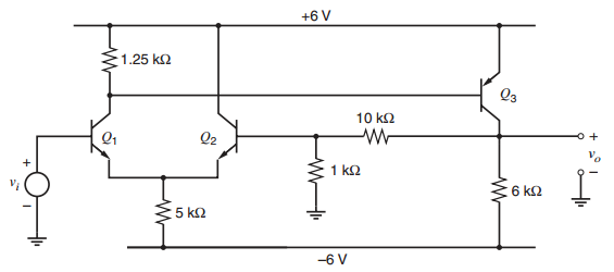
Replace npn transistors Q1€“Q2in Fig. 8.49 with NMOS transistorsM1€“M2, and replace the pnp transistor Q3with PMOS transistor M3. Also, replace the 1.25 k resistor in the drain of M1with a 4.35 kΩ resistor. Repeat the calculations and simulations in Problem 8.13. For
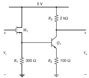
A feedback amplifier is shown in Fig. 8.49. Device data are as follows: βnpn= 200, βpnp= 100, |VBE(on)| = 0.7V, rb= 0, and |VA| = ˆž. If the dc input voltage is zero, calculate the overall gain vo/vi, the loop gain, and the input and output impedance at low
Repeat Problem 8.11 if the output signal is taken as the voltage at the emitter of Q3.Repeat Problem 8.11The half-circuit of a balanced monolithic series-series triple is shown in Fig. 8.18a. Calculate the input impedance, output impedance, loop gain, and overall gain of the half-circuit at low
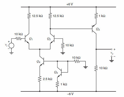
The half-circuit of a balanced monolithic series-series triple is shown in Fig. 8.18a. Calculate the input impedance, output impedance, loop gain, and overall gain of the half-circuit at low frequencies using the following data:RE1 = RE2 = 290 RF = 1.9kΩRL1 = 10.6k RL2 = 6kΩFor the transistors,
Repeat Problem 8.8 using the formulas from return-ratio analysis.Repeat Problem 8.8(a) Repeat Problem 8.7(a) with all NMOS transistors in Fig. 8.48 replaced by bipolar npn transistors. All collector currents are 1 mA and β = 200,VA = 50 V, and rb =0.(b) If the circuit is fed from a
Repeat Problem 8.7 using the formulas from return-ratio analysis.Repeat Problem 8.7The ac schematic of a shunt-shunt feed-back amplifier is shown in Fig. 8.48. All transistors have ID = 1 mA, W/L = 100, k' = 60 μA/V2, and λ = 1/(50 V).(a) Calculate the overall gain
(a) Repeat Problem 8.7(a) with all NMOS transistors in Fig. 8.48 replaced by bipolar npn transistors. All collector currents are 1 mA and β = 200,VA = 50 V, and rb=0.(b) If the circuit is fed from a source resistance of1k in parallel with ii, what is the new output resistance of the
The ac schematic of a shunt-shunt feed-back amplifier is shown in Fig. 8.48. All transistors have ID= 1 mA, W/L = 100, k' = 60 μA/V2, and λ = 1/(50 V).(a) Calculate the overall gain vo/ii, the loop transmission, the input impedance, and the output impedance at low
For the shunt-shunt feedback amplifier of Fig. 8.15a, take RF =100 kΩ and RL = 15 kΩ. For the op amp, assume that Ri =500 kΩ, Ro = 200, and av = 75,000. Calculate input resistance, output resistance, loop transmission, and closed-loop gain:(a) Using the formulas from two-port analysis.(b)
Verify (8.43), (8.44), and (8.45) for a series-series feedback amplifier.(8.43)io/vi = a/1+af(8.44)Zi = zi(1 + T)(8.45)Zo = zo (1 + T)
Verify (8.40), (8.41), and (8.42) for a shunt-series feedback amplifier.(8.40)I0 /ii = a/ 1 + af(8.41)Zi = zi/1 + T(8.42)Z0 = z0 (1 + T)
(a) For the conditions in Problem 8.2(b), sketch the output voltage waveform So and the error volt-age waveform Sε if a sinusoidal input voltage Si with amplitude 1.5 V is applied.(b) Repeat (a) with an input amplitude of 2 V.
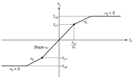
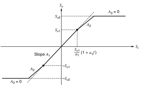
For the characteristic of Fig. 8.2 the following data apply:So2 = 15 V So1 = 7V a1 = 50,000 a2 = 20,000(a) Calculate and sketch the overall transfer characteristic of Fig 8.3 for the above amplifier when placed in a feedback loop with f = 10ˆ’4.(b) Repeat (a) with f = 0.1 S. az = 0
(a) In a feedback amplifier, forward gain α = 100,000 and feedback factor f = 10−3. Calculate overall gain A and the percentage change in A if a changes by 10 percent.(b) Repeat (a) if f = 0.1.
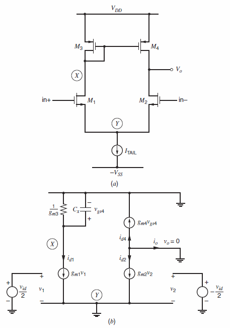
Calculate the pole and zero associated with the current-mirror load in Fig. 7.33 if ID3= ˆ’100 µA, |Vov3| = 0.2 V, and Cx= 0.1 pF.Fig. 7.33: VDD Мз M4 V. х in- M2, in+ M1 ITAIL -Vss (a) g14 Вт3 О ВтаVgs4 is4 i, Vo= 0 Вт2V2 ВтiV1 Vid V2 Vid V1 (b)
Find an expression for Gm(s) = io(s)/Ï…id(s) for the circuit in Fig. 7.33 and verify the equations for the pole and zero given in Section 7.3.5.Fig. 7.33: VDD Мз M4 V. х in- M2, in+ M1 ITAIL -Vss (a) g14 Вт3 О ВтаVgs4 is4 i, Vo= 0 Вт2V2 ВтiV1 Vid V2 Vid V1 (b)
Add a 0.5 pF load capacitor from the output to ground to the integrator in Fig. 7.50. When this capacitor is added, the circuit has a loop of three capacitors. Direct application of the short-circuit time constant method here gives zero for each short-circuit time-constant. The problem here is that
To calculate the dominant pole, calculate the open circuit time constants CinR = 0·2 × 10€“12× 20 × 103= 4 × 10€“9S(a) An integrator is shown in Fig. 7.50. Use zero-value time constants to estimate the dominant pole and
(a) Use zero-value time constants to estimate the dominant pole and short-circuit time constants to estimate the nondominant pole for the common-source amplifier in Problem 7.2.(b) Compare your answers with a SPICE simulation.Data from Prob. 7.2:Repeat Problem 7.1 for the MOS common source stage
(a) For the common-emitter amplifier in Problem 7.1, use zero-value time constants to estimate the dominant pole and short-circuit time constants to estimate the nondominant pole.(b) Compare your estimates with a SPICE simulation.Data from Prob. 7.1:A MOS differential amplifier is shown in Fig.
AMOS cascode stage is shown in Fig. 7.43b. Replace the load resistor with a load capacitor CL= 2 pF. Assume the total capacitance that connects to the drain of M1 can be modeled by a capacitor Cp= 0.2pF from that drain to ac ground. Ignore all other capacitors. Therefore, the gain for this circuit
Use the short-circuit time-constant method to estimate the nondominant pole that originates at the drain nodes of M1and M2in the CMOS folded cascade of Fig. 6.28. Assume the gates of M1A, M2A, M5, M11, and M12are biased from low-impedance points and that a voltage drive is applied at Ï…i.
Repeat Problem 7.40 including short-channel effects with εc= 1.5 × 10⁶V/m.Data from Prob. 7.40:Use the zero-value time-constant method to estimate the small-signal dominant pole for the current gain of the MOS cascode current mirror of Fig. 4.9. Assume an input ac current
Use the zero-value time-constant method to estimate the small-signal dominant pole for the current gain of the MOS cascode current mirror of Fig. 4.9. Assume an input ac current source in parallel with IINand a zero load impedance with Vout= VGS3+ VGS4. The bias current IIN= 100 µA. Compare
For the BiCMOS circuit of Fig. 3.78, use the zero-value time-constant method to estimate the first and second most dominant poles of the circuit. Assume an input voltage drive. Use bipolar transistor data from Fig. 2.32 and MOSFET parameters Cgd= 90 fF, Csb= Cdb= 200 fF, and Cgs= 200 fF at the bias
A CMOS amplifier stage is shown in Fig. 7.49. Select W/L for M1and M5to give Vi= VO= 2.5V dc and |ID| = 100 µA bias in all devices. The minimum value of L and W is 2 µm. Calculate the small-signal, low-frequency gain and the ˆ’3-dB frequency of the stage. Verify with SPICE.
(a) A wideband MOS amplifier stage is shown in Fig. 7.48. Calculate the small-signal, low-frequency gain and use the zero-value timeconstant method to estimate the ˆ’3-dB bandwidth. Use μnCox= 60 µA/V2, tox= 20 nm, Col= 0.3 fF/(µm of gate width), ψo=
A two-stage bipolar amplifier is shown in Fig. 7.47. Calculate the low-frequency, small-signal voltage gain Ï…o/Ï…iand use the zero-value time constant method to estimate theˆ’3-dB frequency. Use a DM half-circuit for the differential pair. Use SPICE to estimate the
A two-stage amplifier is shown in Fig. 7.46. Calculate the low-frequency, small-signal gain and use the zero-value time-constant method to estimate the ˆ’3-dB frequency. Calculate the 10 to 90 percent rise time for a small step input. Use SPICE to determine the ˆ’3-dB frequency
Replace the MOS transistors in the amplifier in Fig. 7.45 with bipolar npn transistors. The emitter area of Q2is four times that of Q1and corresponding bias currents are IC1= 1 mA and IC2= 4 mA. Repeat the calculations in Problem 7.33 using the following data. Data at the operating point: Q1:
The ac schematic of a wideband MOS current amplifier is shown in Fig. 7.45. The W/L of M2is four times that of M1and corresponding bias currents are ID1= 1 mA and ID2= 4 mA. Calculate the low-frequency, small-signal current gain io/iiand use the zero-value time-constant method to estimate the
Repeat Problem 7.31 with n-channel MOS transistors replacing all bipolar transistors. Assume W = 100 µm, Ldrwn= 2 µm, Ld= 0.2 µm, Xd= 0, λ = 0, k€™n= 60 µA/V2, γ = 0, Vt= 1 V, Cox= 0.7 fF/µm2, Col= 0.15 fF/µm, Cj0= 0.4
An amplifier stage is shown in Fig. 7.44.(a) Calculate the low-frequency, small-signal voltage gain Ï…o/Ï…i.(b) Apply the zero-value time-constant method to the DM half-circuit to calculate the ˆ’3-dB frequency of the gain. Data: Ccs0 = 2 pF, Cμ0 = 0.5
Replace the NMOS transistors in Fig. 7.43 with npn transistors. The resulting ac schematics are of a common-emitter stage and a common-emitter€“common-base (cascode) stage. Repeat the calculations in Problem 7.29 using RS= 5 kΩ, RL= 3 kΩ, and the following data.
Repeat Problem 7.27, replacing the bipolar transistors with MOS transistors. Assume that the values of RB1 and RB2 set ID5 = 1 mA. Use W1 = W2 = W5 = W6 = 100 µm, W3 = W4 = 50 µm, and Ldrwn = 2 µm. See Problem 7.26 for all other MOS transistor data.Data from Prob. 7.26:NMOS data: Vtn = 1 V,
A differential circuit employing active loads is shown in Fig. 7.42. Bias voltage VBis adjusted so that the collectors of Q1and Q2are at +5 V dc. Biasing resistors are RB1= 10 kΩ and RB2= 20 kΩ. Calculate the low-frequency, small-signal voltage gain
Repeat Problem 7.25 with the following changes:1. Replace Q1 with a p-channel MOS transistor, M1. Replace Q2 and Q3 with n-channel MOS transistors, M2 and M3.2. Add a resistor of value 1/gm1 from the gate to the source of M1.3. Take VSUPPLY = 2.5 V.4. Use the formula for Cdb0 given in Problem
An amplifier stage is shown in Fig. 7.41 where bias current IBis adjusted so that VO= 0 V dc. Take VSUPPLY= 10 V.(a) Calculate the low-frequency, small-signal trans-resistance Ï…o/ii and use the zero-value time-constant method to estimate the ˆ’3-dB frequency. Data: npn:
Repeat Problem 7.21 if a bleed resistor of 15 kΩ is added from the emitter of Q1to ground, which increases the collector bias current in Q1to 50 µA.A Darlington stage and a common-collector€“common-emitter cascade are shown schematically in Fig. 7.40, where RS = 100
Replace the bipolar transistors in Fig. 7.40 with NMOS transistors. Repeat the calculations inProblem 7.21, using RS = 100 kΩ, RL = 3 kΩ, and the NMOS transistor model data in Problem 7.2, but use Cdb = 200 fF and Csb = 180 fF here. Take ID1 = 50 µA and ID2 = 1 mA.Data
Repeat Problem 7.21 if the input signal is a current source of value iiapplied at the base of Q1. (That is, iireplaces the voltage source Ï…iand resistance RS.) The transfer function is then a trans-resistance Ï…o/ii.Data from Prob. 7.21:A Darlington stage and a
A Darlington stage and a common-collector€“common-emitter cascade are shown schematically in Fig. 7.40, where RS= 100 kΩ and RL= 3 kΩ.(a) Calculate the low-frequency small-signal voltage gain Ï…o/Ï…i for each circuit.(b) Use the zero-value
Repeat Problem 7.18 if a resistor of value 50 kΩ is connected between drain and gate of the transistor.Data from Prob. 7.18:Repeat Problem 7.14 using a NMOS transistor in place of the bipolar transistor. Use ID = 0.5mA and the transistor data in Problem 7.2.Data from Prob. 7.14:The ac
Repeat Problem 7.18 if a 900 source-degeneration resistor is included in the circuit.Data from Prob. 7.18:Repeat Problem 7.14 using a NMOS transistor in place of the bipolar transistor. Use ID = 0.5mA and the transistor data in Problem 7.2.Data from Prob. 7.14:The ac schematic of a common-emitter
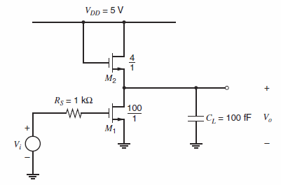
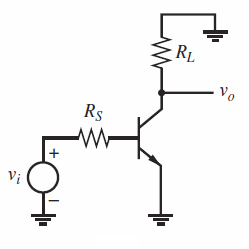
Repeat Problem 7.14 using a NMOS transistor in place of the bipolar transistor. Use ID= 0.5mA and the transistor data in Problem 7.2.Data from Prob. 7.14:The ac schematic of a common-emitter stage is shown in Fig. 7.2a. Calculate the low-frequency small-signal voltage gain
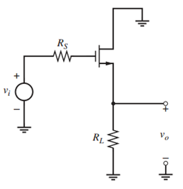
Repeat the calculations in Problem 7.14 for the common-source stage in Fig. 7.2b. Take VDB= 7.5 V and ID= 0.5 mA. Use the same transistor data and resistor values as in Problem 7.2 with the following exceptions:1. Cox and Cgd are not given, but fT = 3 GHz.2. Cdb is not equal to 0. Calculate the
Repeat Problem 7.14 if an emitter degeneration resistor of value 300 is included in the circuit.Data from Prob. 7.14:The ac schematic of a common-emitter stage is shown in Fig. 7.2a. Calculate the low-frequency small-signal voltage gain Ï…o/Ï…i and use the zerovalue
Repeat Problem 7.12 for a NMOS commongate stage using RL = 0 and RS = ∞. Use ID = 0.5 mA and the MOS transistor data in Problem 7.2. Plot the impedance magnitudes from f = 100 kHz to f = 100 GHz.Data from Prob. 7.12:A common-base stage has the following parameters: IC = 0.5 mA, Cπ = 10 pF, Cμ =
A common-base stage has the following parameters: IC = 0.5 mA, Cπ = 10 pF, Cμ = 0.3 pF, rb = 200 Ω, β = 100, ro = ∞, RL = 0, and RS = ∞.(a) Calculate an expression for the small-signal current gain of the stage as a function of frequency and thus determine the frequency where the current
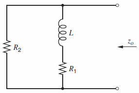
(a) Find expressions for R1, R2, and L in the output impedance model for a MOS source follower assuming RS ≫ 1/gm, γ ≠ 0, and υsb = υo.(b) Plot the magnitude of the output impedance versus frequency from f = 10 kHz to f = 10 GHz, using log scales, when RS = 1 M, gm = 0.3
For the source follower in Fig. 7.13b, find the low-frequency gain and plot the magnitude and phase of its voltage gain versus frequency from f = 10 kHz to f = 20 GHz, using log scales. Compare your plot with a SPICE simulation. Use the transistor data given in Problem 7.2 with a resistive load of
Calculate the values of the elements in the small-signal equivalent circuits for the input and output impedances of the emitter follower of Problem 7.8. Sketch the magnitudes of these impedances as a function of frequency from f = 10 kHz to f = 20 MHz, using log scales. Use SPICE to determine the
A lateral pnp emitter follower has RS = 250 Ω, b = 200 Ω, β = 50, IC = −300 µA, fT = 4 MHz, RE = 4 kΩ, Cμ = 0, and ro = ∞. Calculate the small-signal voltage gain as a function of frequency. Sketch the magnitude of the voltage gain in decibels from f = 10 kHz to f = 20 MHz, using a log
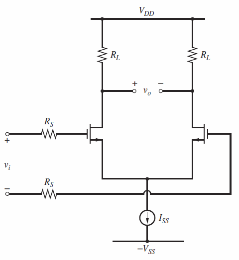
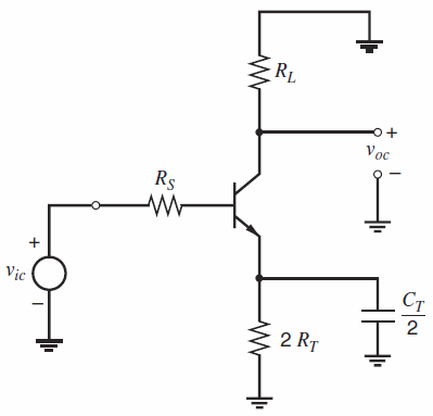
A MOS differential amplifier is shown in Fig. 7.9. For this circuit, carry out the calculations in Problem 7.6. Use ISS= 1 mA, the values of RT= 300 kΩ and CT= 2 pF as defined in Fig. 7.11b, and the transistor data in Problem 7.2.Fig. 7.9:Fig. 7.11 b: VDD RL RL Rs Vị Rs Iss -V ss RL
A bipolar differential amplifier as shown in Fig. 7.5 has IEE= 1 mA. The resistor values and transistor data are as given in Problem 7.1. If the tail current source has an associated resistanceRT= 300 kΩ and capacitance CT= 2 pF as defined in Fig. 7.11a, calculate the CM and DM gain and
Showing 100 - 200
of 376
1
2
3
4
Step by Step Answers