New Semester
Started
Get
50% OFF
Study Help!
--h --m --s
Claim Now
Question Answers
Textbooks
Find textbooks, questions and answers
Oops, something went wrong!
Change your search query and then try again
S
Books
FREE
Study Help
Expert Questions
Accounting
General Management
Mathematics
Finance
Organizational Behaviour
Law
Physics
Operating System
Management Leadership
Sociology
Programming
Marketing
Database
Computer Network
Economics
Textbooks Solutions
Accounting
Managerial Accounting
Management Leadership
Cost Accounting
Statistics
Business Law
Corporate Finance
Finance
Economics
Auditing
Tutors
Online Tutors
Find a Tutor
Hire a Tutor
Become a Tutor
AI Tutor
AI Study Planner
NEW
Sell Books
Search
Search
Sign In
Register
study help
sciences
digital systems design
Digital Systems Design Using Verilog 1st edition Charles Roth, Lizy K. John, Byeong Kil Lee - Solutions
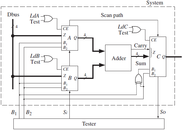
In the system of Figure 10-33, A, B, and C are BILBO registers. The B1and B2inputs to each of the registers determine its BILBO operating mode as follows:B1B2= 00, shift register; B1B2= 01, PRPG (pattern generator); B1B2= 10, normal system mode; B1B2= 11, MISR (signature register). The shifting
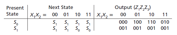
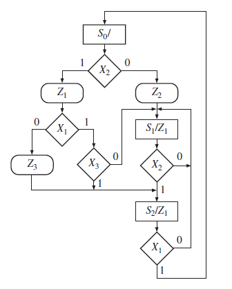
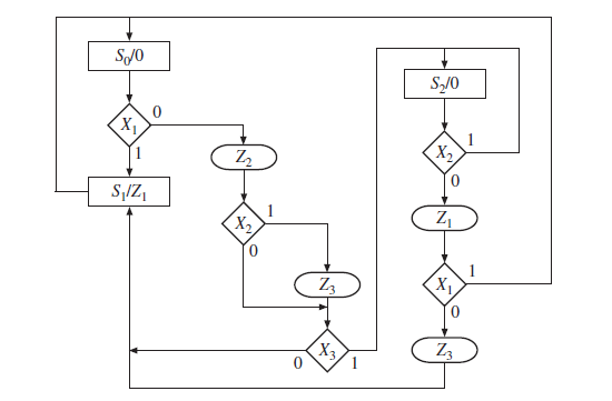
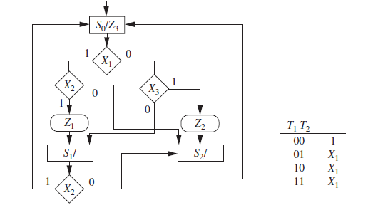
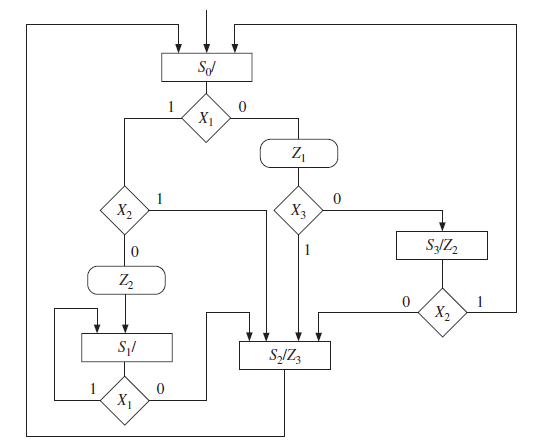
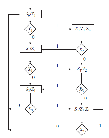
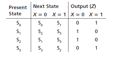
Construct an SM chart that is equivalent to the following state table. Test only one variable in each decision box. Try to minimize the number of decision boxes. Show Mealy and Moore outputs on the SM chart. Output (Z,Z,Z,) 11 Next State X,X, = 00 01 S, S, S, S, S, S, S, So Present State 10 11 X,X2
Write a test bench for the elevator controller of Problem 5.10. The test bench has two functions: to simulate the operation of the elevator (including the door operation) and to provide a sequence of button pushes to test the operation of the controller.To simulate the elevator: if the elevator is
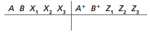
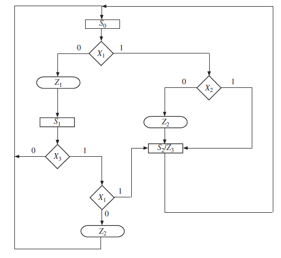
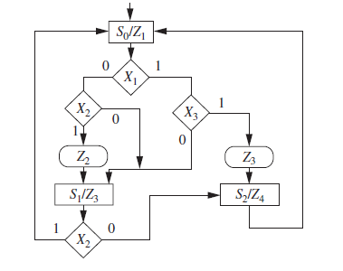
For the following SM chart,(a) Draw a timing chart that shows the clock, the state (S0, S1, or S2), the inputs (X1, X2, and X3), and the outputs. The input sequence is X1 X2 X3 = 011, 101,111,010,110,101,001. Assume that all state changes occur on the rising edge of the clock and the inputs change
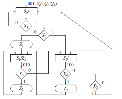
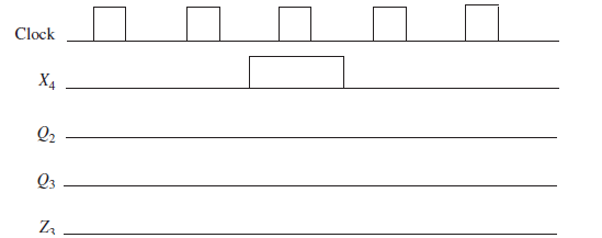
For the given SM chart,(a) Complete the following timing diagram (assume that X1 = 1, X2 = 0, X3 = 0, X5 = 1, and X4 is as shown). Flip-flops change state on falling edge of clock.(b) Using the given one-hot state assignment, derive the minimum next state and output equations by inspection of
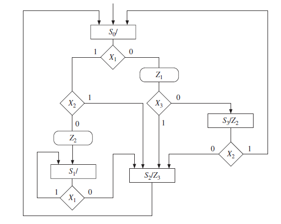
(a) Draw an SM chart that is equivalent to the state graph of Figure 4-46.(b) If the SM chart is implemented using a PLA and three flip-flops (A, B, C), give the PLA-table (state transition table). Use a straight binary state assignment.(c) Give the equation for A+determined by inspection of the
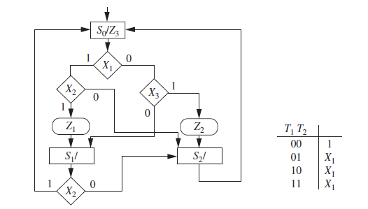
(a) Write Verilog code that describes the following SM chart. Assume that state changes occur on the falling edge of the clock. Use two processes(b) The SM chart is to be implemented using a PLA and two flip-flops (A and B). Complete the state transition table (PLA table) by tracing link paths.
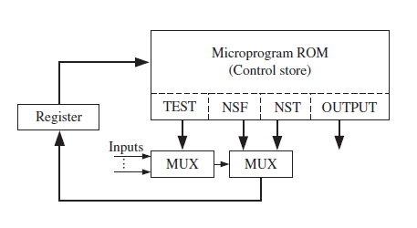
Realize the following SM chart using a ROM with a minimum number of inputs, a multiplexer, and a loadable counter (like the 74163). The ROM should generate NST. The multiplexer inputs are selected as shown in the table beside the SM chart.(a) Draw the block diagram.(b) Convert the SM chart to the
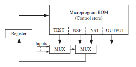
Realize the SM chart of Problem 5.16 using the two-address microprogramming structure shown in Figure 5-29.(a) Convert the SM chart to the proper form by adding a minimum number of states to the given chart.(b) Write the microprogram required to implement the circuit.(c) What is the size of the ROM
The following SM chart is to be realized using the two-address microprogramming structure shown in Figure 5-29.(a) Convert the SM chart to the proper form by adding a minimum number of states to the given diagram. Make a suitable state assignment.(b) Write the microprogram required to implement
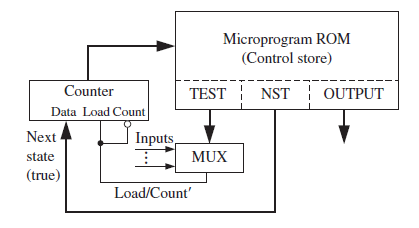
(a) What are the conditions an SM chart must satisfy in order to realize it using single-address microprogramming with a counter, a ROM, and a multiplexer as in Fig 5-33?Figure 5-33: Microprogrammed System with Single- Address Microcode(b) Give the modified SM chart and the required state
Realize the SM chart given here using a ROM, a counter, and a 4-to-1 multiplexer. (a) Draw a block diagram. Show the MUX inputs.(b) Change the SM chart to the proper form. Mark required changes on the following chart.(c) Make a suitable state assignment. Give the first six rows of the ROM
Realize the SM chart of Problem 5.20 using the two-address microprogramming hardware structure shown in Figure 5-29.(a) Convert the SM chart to the proper form by adding a minimum number of states to the given diagram. What are the changes needed?(b) Write the microcode for implementing this state
The following SM chart is to be realized using single-address microprogramming.(a) Show the new SM chart and show the state assignments. The MUX inputs are 1, X1, X2, and X3. Do not invert inputs. Add extra states if necessary.(b) Write the microcode for implementing this state machine using
Given the following ASM chart,(a) Derive the next state and output equations, assuming the following state assignment:S0 = 00, S1 = 01, S2 = 10.(b) Convert the ASM chart to a form where it can be implemented by singleaddress microprogramming, with only next state true (NST) specified in the
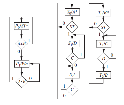
The SM charts for three linked machines are given here. All state changes occur during the falling edge of a common clock. Complete a timing chart including ST, Wa, A, B, C, and D. All state machines start in the state with an asterisk (*). SJA* TJB* P/ST* (ST (ST A+B S,ID TIC 1 D P/Wa Тув A•B
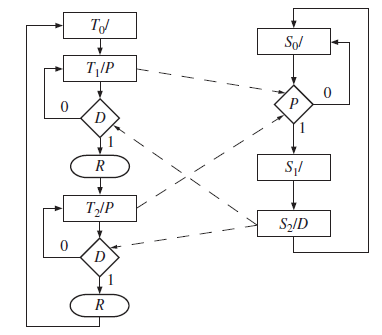
SM charts for two linked state machines are shown here. Machine T starts in state T0, and machine S starts in state S0. Draw a timing chart that shows CLK, the states of T and S, and signals P, R, and D for 10 clocks. All state changes occur on the rising edge of the clock. TJ Sol T,IP 1. S/ T/P SID
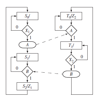
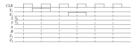
The SM charts for two linked state machines are given in the following diagram.(a) Complete the timing diagram shown here.(b) For the SM chart on the left, make a one-hot state assignment and derive D flip-flop input equations and output equations by inspection. TJZ, Sd (X1 A 1 T/ X, SIZ, CLK X1
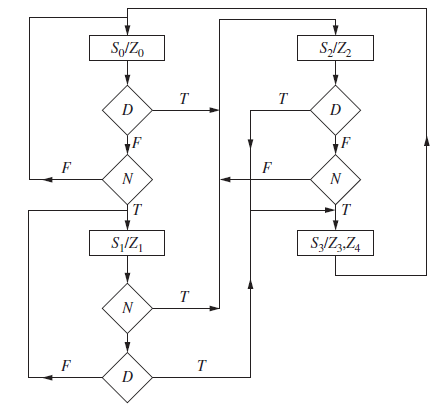
The SM chart for a simplified vending machine is shown here. The vending machine accepts only dimes and nickels. One soda costs 15 cents at this vending machine.D:Dime N:Nickel Z0:0cent Z1:5cents Z2:10cents Z3:15cents Z4:soda(a)
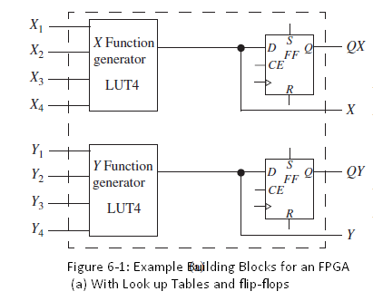
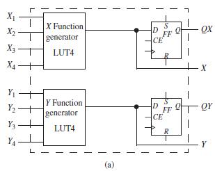
An 8-bit right-shift register with parallel load is to be implemented using an FPGA with logic blocks as shown in Figure 6-1(a). The flip-flops are labeled X7X6X5X4X3X2X1X0. The control signals N and S operate as follows: N = 0, do nothing; NS = 11, right shift; NS = 10, load. The serial input for
Implement a 2-bit binary counter using one logic block as shown in Figure 6-1(a). A0is the least significant bit, and A1is the most significant bit of the counter. The counter has a synchronous load (Ld). The counter operates as follows: En = 0 No change. En = 1, Ld = 1 Load A0and A1with external
Design a 4-bit right-shift register using an FPGA with logic blocks as shown in Figure 6-1(a). When the register is clocked, the register loads if Ld = 1 and En = 1; it shifts right when Ld = 0 and En = 1; and nothing happens when En = 0. Si and So are the shift input and output of the register.
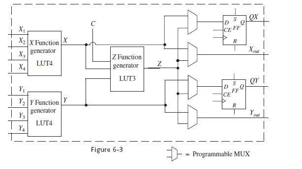
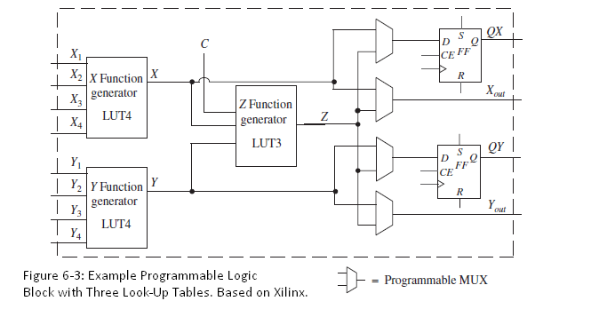
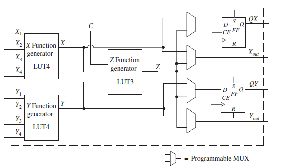
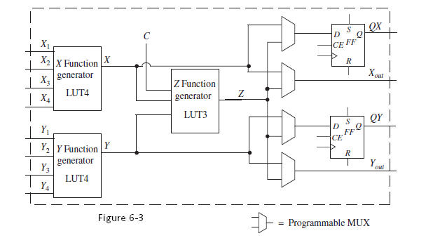
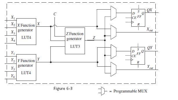
The next-state equations for a sequential circuit with two flip-flops (Q1and Q2), input signals R, S, T, and an output P areD1 = Q1+ = Q2R1 Q1S D2 = Q2+ = Q1+ Q2'TThe output equation is P = Q2RT + Q1ST(a) Explain how this sequential circuit can be implemented using a single Figure 6-3 logic
(a) Implement an 8-to-1 multiplexer using a minimum number of logic blocks of the type shown in Figure 6-1(a). Give the X and Y functions for each block and show the connections between blocks.(b) Repeat (a) using the logic blocks of Figure 6-3. Give X, Y, and Z for each block.(c) What are the LUT
(a) Write Verilog code that describes the logic block shown in Figure 6-1(a). Use the following module:module Figure6_1a(X_in,Y_in,clk,CE,Qx,Qy,X,Y,XLUT,YLUT);input[1:4]X_in,Y_in;input CE,clk;input[0:15] XLUT,YLUT;inout X,Y;output Qx,Qy;...endmoduleFigure 6-1(a)(b) Write structural Verilog code
(a) Write Verilog code that describes the logic block shown in Figure 6-3. Use a module similar to that used in Problem 6.6(a), except add ZLUT and SA, SB, SC, and SD. SA, SB, SC, and SD represent the programmable select bits that control the four MUXes. These bits should be assigned values of 0 or
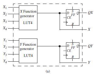
(a) How many logic blocks as shown in Figure 6-1(a) are required to create a 4-to-16 decoder?(b) Give the contents of the LUTs in the first logic block.Figure 6-1(a) X X Function QX D FF CE X2 generator X - LUT4 X4- Y - Y Function generator to Y2 - D FF QY CE Y3 – LUT4 YA Y L (a) L.
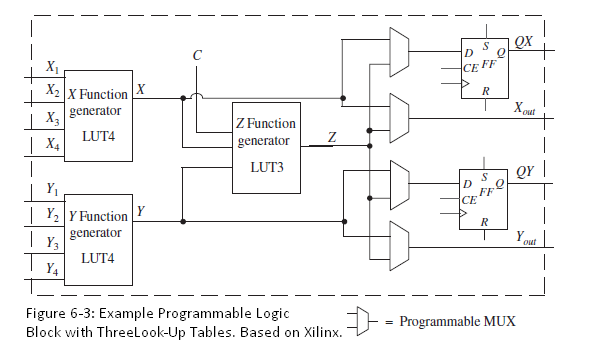
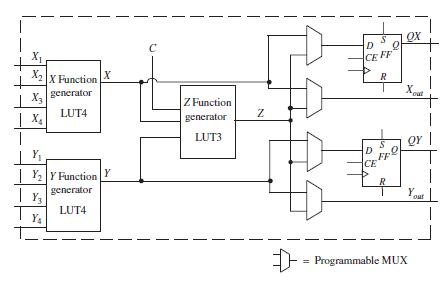
(a) How many logic blocks as shown in Figure 6-3 are required to create an 8-to-3 priority encoder?(b) Give the contents of the LUTs in the first logic block. Qх х, CE FF X2X Function Xout | X generator LUT4 | X4 Z Function generator LUT3 Qr | | Yı CE | Y2 Y Function generator Y3 out LUT4
Show how to realize the following combinational function using two Figure 6-1(a) logic blocks. Show the connections on a copy of Figure 6-1(a) and give the functions X and Y for both blocks.F = X1'X2X3'X6 + X2'X3'X4X6' + X2X3'X4' + X2X3X4'X6 + X3'X4X5X6' + X7Figure 6-1(a) X X Function QX D FF CE X2
Realize the following next-state equation using a minimum number of Figure 6-1(a) logic blocks. Draw a diagram that shows the connections to the logic blocks and give the functions X and Y for each cell. (The equation is already in minimum form.) Q+ = UQV'W + U'Q'VX'Y' + UQX'Y + U'Q'V'Y +
Show how to realize the following next-state equations using a minimum number of the Kintex logic slice. Draw a diagram to show the connections between the logic elements and indicate how many CLBs you have used.Q1+ = X1'X2'Q1 + Q2 X3X4Q2+ = X3X2Q1 + X1'Q3Q3+ = X4Q2 C = X1'Q2 Q3Q1'
What is the minimum number of Figure 6-3 logic blocks required to realize the following function?X = X1'X2'X3'X4'X5 + X1X2X3X4X5 + X5'X6X7'X8'X' + X5'X6'X7X8X9'If your answer is 1, show the required input connections on a copy of Figure 6-3 and mark the internal connection paths with heavy lines.
Illustrate how to realize the following equations using a minimum number of the Stratix IV logic module. Display the input/output by drawing a diagram and highlight the data path on the diagram. X+ = A’BY + E’FX + B’E + A’F’; Y+ = A’D’X’ + BC + AB’C’G; Z+
Given Z(T, U, V, W, X, Y) = VW'X + U'V'WY + TV'WY',(a) Show how Z can be realized using a single Figure 6-3 logic block. Show the cell inputs on a copy of Figure 6-3; indicate the internal connections in the cell; and specify the functions X, Y, and Z.Figure 6-3(b) Show how Z can be
Decompose the following function using Shannon’s decomposition around the variable X6. Do not simplify the function.F = X1’X2X3’X4X6 + X2’X3’X4X6’ + X2’X4’ + X3X4X5X6 + X3’X4X6’ + X1X3Write an expression for F in terms of the decomposed functions and X6.
Use Shannon’s expansion theorem around a and b for the function.Y = abcde + cde’f + a’b’c’def + bcdef ‘ + ab’cd’ef’ + a’bc’de’f + abcd’e’f.so that it can be implemented using only 4-variable function generators. Draw a block diagram to indicate how Y
Use Shannon’s expansion theorem around e and f for the functionY = ab’cdef + a’bc’d’e + b’c’ef’ + abcde’fso that it can be implemented using a minimum number of 4-variable functions. Rewrite Y to indicate how it will be implemented using 4-variable function
(a) Use Shannon's expansion theorem around a for the functionY = ab'cd'e + a'bc'd'e + b'c'e + abcdeso that it can be implemented using 4-variable functions.(b) Use the expanded function to show how Y can be implemented using one Figure 6-3 logic block. Mark (highlight) the input signals and the
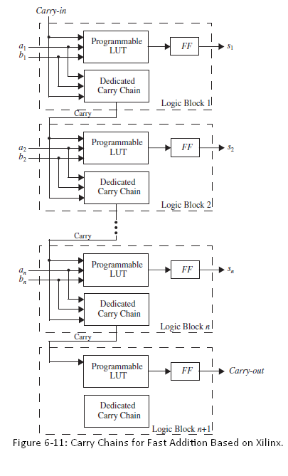
(a) If logic blocks of Figure 6-1(a) are used, how many LUTs are required to build a 4-bit adder with accumulator?(b) If an FPGA with built-in carry-chain logic as shown in Figure 6-11 is used, how many 4-input LUTs are required?(c) Design a 4-bit adder-subtracter with accumulator using an FPGA
A 4 ⊗ 4 array multiplier (Figure 4-29) is to be implemented using an FPGA. (a) Partition the logic so that it fits in a minimum number of Figure 6-1(a) logic blocks. Draw loops around each set of components that will fit in a single logic block. Determine the total number of 4-input LUTs
(a) Use Shannon’s expansion theorem to expand the following function around A and then expand each sub-function around D:Z = AB’CD’E’F + A’BC’D’EF’ + B’C’E’F + A’BC’E’F’ + ABCDE(b) Explain how the expanded function could be implemented using two Xilinx Kintex FPGA
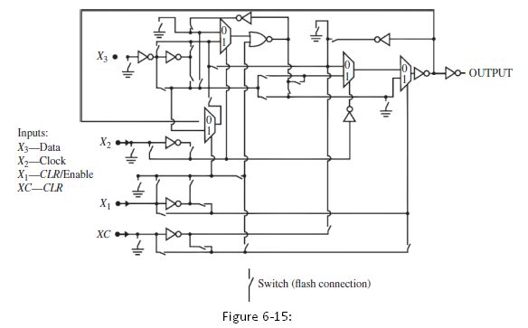
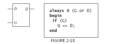
(a) Indicate the connections of the switches in Figure 6-15 to realize the functionF = AB + A€™C(b) Indicate the connections of the switches in Figure 6-15 to realize a latch as shown in Figure 2-18.(c) Indicate the connections of the switches in Figure 6-15 to realize a D-flip-flop. X3
The logic equations for a sequential network with five inputs, two flip-flops, and two outputs areQ1+ = Q1(Q2ABC) + Q1’(Q2’CDE)Q2+ = Q1’Z1 = Q1’Q2’AB + Q1’Q2’A’B’ + Q1Q2’AB’ + Q1Q2(A’ + B + C)Z2 = Q1A’ + Q1B + Q2’How many Kintex slices are required to implement the logic
Stratix IV and Stratix V are the popular Altera FPGAs on the market. Indicate the most significant differences between these chips’ logic modules
Show how 32 × 32-bit unsigned multiplication can be accomplished using four 16 × 16-bit multipliers and several adders. Draw a block diagram showing the required connections.
Fast shifting can be accomplished by using dedicated multipliers. Shifting left N places is equivalent to multiplying by 2N.(a) Given that A is a 16-bit unsigned number and 0 ≤ N ≤ 15, show how to construct a left shifter using a multiplier and a decoder.(b) Write Verilog code that infers this
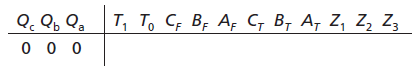
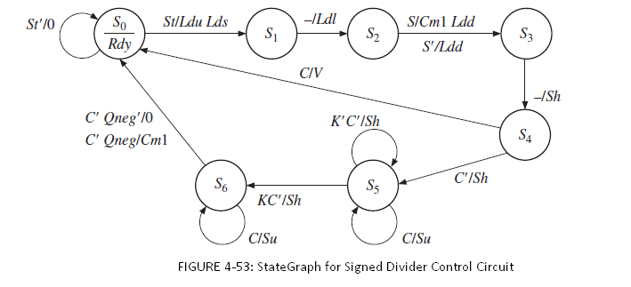
Make a one-hot state assignment for Figure 4-53 and write the next-state and output equations by inspection. Then change the state assignment so that S0is assigned 0000000, S1is assigned 1100000, S2is 1010000, and so forth and rewrite the equa-tions for this assignment. -HLdl SICM1 Ldd S2
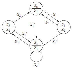
For the given state graph:(a) Derive the simplified next-state and output equations by inspection. Use the following one-hot state assignment for flip-flopsQ0Q+Q2Q3; S0, 1000; S1, 0100; S2, 0010; S3, 0001.(b) How many Kintex slices (Figure 6-13) are required to implement these equations? So X1 X4
Consider the Verilog codemodule example(a,b);input[1:0] a;output[1:0] b;reg[1:0] b;always @(a)begincase(a)0: b 5 2’d3;1: b 5 2’d2;2: b 5 2’d1;3: b 5 2’d1;endcaseendendmodule(a) Show the hardware you would obtain if you synthesize the foregoing Verilog code without any optimizations. Explain
Draw the hardware structures that will be inferred by typical synthesizers from the code excerpts that follow. A, B, and E are 4-bit vectors, and C and D are 2-bit numbers; clock is a 1-bit signal. Draw the structure and mark the inputs and outputs.(a) always @(clock)beginA <= {A[3], A[3:1]};B
(a) Draw a logic diagram (use gates, adders, MUXes, D flip-flops, etc.) that shows the result of synthesizing the following Verilog code. A, B, and C are 3-bitunsigned vectors.always @(negedge CLK)beginif(C0 == 1)C <= ~A;if(Ad == 1)C <= A + B;if(Sh == 1)C <= C >>> 1;end(b)
Draw the hardware structures that will be inferred by typical synthesizers from the code excerpts that follow. If any ambiguities exist in the code, mention what you are assuming. Show optimized and unoptimized hardware.(a) always @(a)begincase(a)0: b = 2;1: b = 0;2: b = 3;3: b = 1;endcaseend(b)
What hardware does the statementF = (A >= B);result in? Assume that A and B are 8-bit vectors.
Generate optimized hardware for the following statement, assuming A is a 4-bit vector: F = (A = 9);
(a) What is the biggest number that can be represented in the 8-bit 2’s complement floating-point format with 4 bits for exponent and 4 for fraction?(b) What is the smallest number that can be represented in the 8-bit 2’s complement format with 4 bits for exponent and 4 for fraction?(c) What is
Convert the following decimal numbers in the IEEE single precision format:(i) 25.25, (ii) 2000.22, (iii) 1, (iv) 0, (v) 1000, (vi) 8000, (vii) 106, (viii) -5.4,(ix) 1.0 x 2-140, (x) 1.5 x 10⁹
Convert the following decimal numbers to IEEE double precision format:(i) 25.25, (ii) 2000.22, (iii) 1, (iv) 0, (v) 1000, (vi) 8000, (vii) 106, (viii) -5.4,(ix) 1.0 x 2-140, (x) 1.5 x 10⁹
What do the following hex representations mean if they are in IEEE single precision format?(i) ABABABAB, (ii) 45454545, (iii) FFFFFFFF, (iv) 00000000, (v) 11111111,(vi) 01010101
What do the following hex representations mean if they are in IEEE double precision format?(i) ABABABAB 00000000, (ii) 45454545 00000001, (iii) FFFFFFFF 10001000,(iv) 00000000 00000000, (v) 11111111 10001000, (vi) 01010101 01010101
(a) Represent -35.25 in IEEE single precision floating-point format. (b) What does the hex number ABCD0000 represent if it is in an IEEE single precision floating-point format?
(a) Represent 25.625 in IEEE single precision floating-point format.(b) Represent -15.6 in IEEE single precision floating-point format.
(a) Multiply the following two floating-point numbers to give a properly normalized result. Assume 4-bit 2’s complement format.F1 = 1.011, E1 = 0101, F2 = 1.001, E2 = 0011(b) Repeat (a) for F1 = 1.011, E1 = 1011, F2 = 0.110, E2 = 1101
A floating-point number system uses a 4-bit fraction and a 4-bit exponent with negative numbers expressed in 2’s complement. Design an efficient system that will multiply the number by -4 (minus four). Take all special cases into account and give a properly normalized result. Assume that the
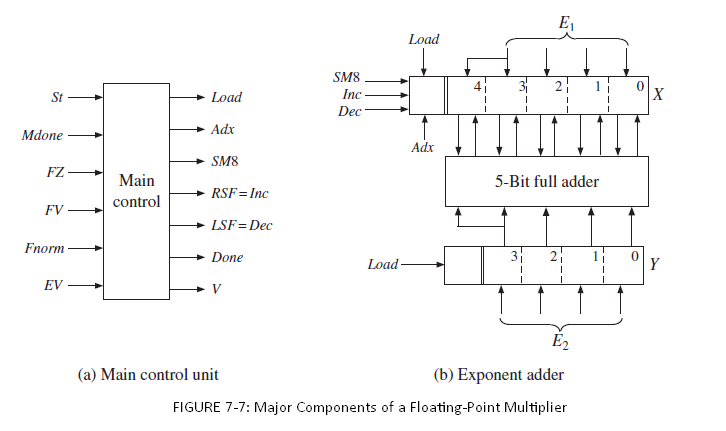
Redesign the floating-point multiplier in Figure 7. 7 using a common 5-bit full adder connected to a bus instead of two separate adders for the exponents and fractions.(a) Redraw the block diagram, being sure to include the connections to the bus, and include all control signals.(b) Draw a new SM
This problem concerns the design of a circuit to find the square of a floating-point number, F x 2E. F is a normalized 5-bit fraction, and E is a 5-bit integer; negative numbers are represented in 2’s complement. The result should be properly normalized. Take advantage of the fact that (-F)2
Write a behavioral Verilog code for a floating-point multiplier using the IEEE single precision floating-point format. Use an overloaded multiplication operator instead of using an add-shift multiplier. Ignore special cases such as infinity, denormalized, and not-a-number formats. Truncate the
Add the following floating-point numbers (show each step). Assume that each fraction is 5 bits (including sign) and each exponent is 5 bits (including sign) with negative numbers in 2’s complement. F1 = 0.1011 E1 = 11111F2 = 1.0100 E2 = 11101
Two floating-point numbers are added to form a floating-point sum:(F1 x 2E1) + (F2 x 2E2) = F x 2EAssume that F1 and F2 are normalized and the result should be normalized.(a) List the steps required to carry out floating-point addition, including all special
For the floating-point adder of Figure 7-14, modify the Verilog code so that(a) It handles IEEE standard single precision denormalized numbers both as input and output.(b) In state 2, it speeds up the processing when the exponents differ by more than 23.(c) It rounds up instead of truncating the
a) Perform the floating point addition.b) Draw an SM chart for a floating-point adder that adds F1 x 2E1 and F2 x 2E2. Assume that the fractions are initially normalized (or zero) and the final result should be normalized (or zero). A zero fraction should have an exponent of -8. Set an exponent
(a) Draw a block diagram for a floating-point subtracter. Assume that the inputs to the subtracter are properly normalized, and the answer should be properly normalized. The fractions are 8 bits including sign, and the exponents are 5 bits including sign. Negative numbers are represented in 2’s
(a) State the steps necessary to carry out floating-point subtraction, including special cases. Assume that the numbers are initially in normalized form and the final result should be in normalized form.(b) Subtract the following (fractions are in 2’s complement): (1.0111 x 2-3) - (1.0101 3
This problem concerns the design of a divider for floating-point numbers:(F1 x 2E1)/(F2 x 2E2) = F x 2E Assume that F1 and F2 are properly normalized fractions (or 0), with negative fractions expressed in 2’s complement. The exponents are
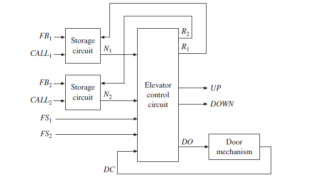
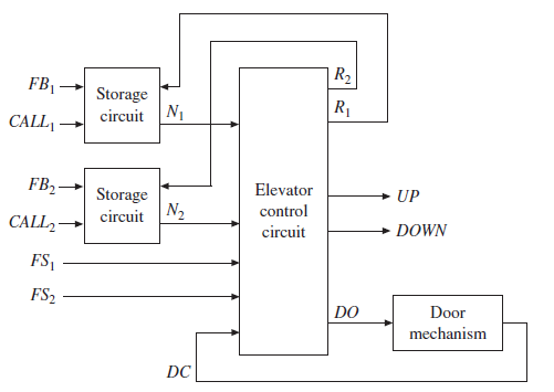
The block diagram for an elevator controller for a building with two floors is shown in the following diagram. The inputs FB1and FB2are floor buttons in the elevator. The inputs CALL1and CALL2are call buttons in the hall. The inputs FS1and FS2are floor switches that output a 1 when the elevator is
Design a multiplier for 16-bit binary integers. Use a design similar to Figures 4-33 and 4-34.(a) Draw the block diagram. Add a counter to the control circuit to count the number of shifts.(b) Draw the SM chart for the controller (three states). Assume that the counter outputs K = 1 after 15 shifts
Design a binary-to-BCD converter that converts a 10-bit binary number to a 3-digit BCD number. Assume that the binary number is ≤ 999. Initially the binary number is placed in register B. When an St signal is received, conversion to BCD takes place and the resulting BCD number is stored in the A
Draw an SM chart for the binary multiplier of Problem 4.22.Data from Problem 4.22.Design a multiplier that will multiply two 16-bit signed binary integers to give a 32-bit product. Negative numbers should be represented in 2’s complement form. Use the following method: First complement the
Draw an SM chart for the square root circuit of Problem 4.14.Data from Problem 4.14.This problem involves the design of a circuit that finds the square root of an 8-bit unsigned binary number N using the method of subtracting out odd integers. To find the square root of N, we subtract 1, then 3,
Draw an SM chart for the BCD-to-binary converter of Problem 4.13.Data from Problem 4.13.This problem involves the design of a BCD-to-binary converter. Initially a 3-digit BCD number is placed in the A register. When an St signal is received, conversion to binary takes place and the resulting binary
(a) Draw the block diagram for a divider that divides an 8-bit dividend by a 5-bit divisor to give a 3-bit quotient. The dividend register should be loaded when St = 1.(b) Draw an SM chart for the control circuit.(c) Write a Verilog description of the divider based on your SM chart. Your Verilog
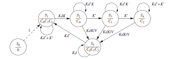
An association has 15 voting members. Executive meetings of this association can be held only if more than half (i.e., at least eight) of the members are present (i.e., eight is the minimum quorum required to hold meetings). Classified matters can be discussed and voted on only if two-thirds of the
Find a minimum-row PLA table to implement the following sets of functions:(a) f1 (A, B, C, D) = ∑m(0, 2, 3, 6, 7, 8, 9, 11, 13), f2 (A, B, C, D) = ∑m(3, 7, 8, 9, 13), f3 (A, B, C, D) = ∑m(0, 2, 4, 6, 8, 12, 13)(b) f1 (A, B, C, D) = cd + ad + a'bc'd', f2 (A, B, C, D) =
(a) Find a minimum-row PLA table to implement the following equations:x (A, B, C, D) = ∑m(0, 1, 4, 5, 6, 7, 8, 9, 11, 12, 14, 15)y (A, B, C, D) = ∑m(0, 1, 4, 5, 8, 10, 11, 12, 14, 15)z (A, B, C, D) = ∑m(0, 1, 3, 4, 5, 7, 9, 11, 15)(b) Indicate the connections that will be made to program a
A D flip-flop has a setup time of 5 ns, a hold time of 3 ns, and a propagation delay from the rising edge of the clock to the change in flip-flop output in the range of 6 to 12 ns. An OR gate delay is in the range of 1 to 4 ns.(a) What is the minimum clock period for proper operation of the
What is the size of the smallest ROM that is needed to implement the following?(a) An 8-bit full adder (assume carry-in and carry-out)(b) A BCD-to-binary converter (2 BCD digits)(c) A 4-to-1 MUX(d) A 32-bit adder (adds two 32-bit numbers to give a 33-bit sum)(e) A 3-to-8 decoder(f) A 32-bit adder
Given F = A'B' + BC' and G = AC + B', write a complete Verilog module that realizes the functions F and G using an 8-word x 2-bit ROM. Include the array type declaration and the constant declaration that defines the contents of the ROM.
Implement the following state table using a ROM and two D flip-flops. Use a straight binary state assignment. (a) Show the block diagram and the ROM truth table. Truth table column headings should be in the order Q1 Q0 X D1 D0 Z.(b) Write Verilog code for the implementation. Use an array
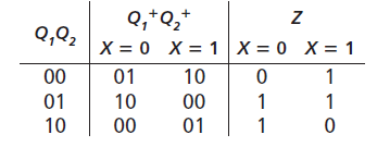
The following state table is implemented using a ROM and two D flip-flops (falling edge triggered):(a) Draw the block diagram.(b) Write Verilog code that describes the system. Assume that the ROM has a delay of 10ns and each flip-flop has a propagation delay of 15ns. Q,+Q,* X = 0 X = 1 Q,Q2 X = 0 X
Find a minimum-row PLA to implement the following three functions:f (A, B, C, D) = ∑m(3, 6, 7, 11, 15)g (A, B, C, D) = ∑m(1, 3, 4, 7, 9, 13)h (A, B, C, D) = ∑m(4, 6, 8, 10, 11, 12, 14, 15)Use Karnaugh maps to find common terms. Give the logic equations with common terms underlined, the PLA
Write VHDL code that describes the output macrocell of a 22V10. The entity should include S1 and S0. The flip-flop has an asynchronous reset (AR) and a synchronous preset (SP).
An N-bit bidirectional shift register has N parallel data inputs, N outputs, a left serial input (LSI), a right serial input (RSI), a clock input, and the following control signals:Load: Load the parallel data into the register (load overrides shift).Rsh: Shift the register right (LSI goes
Show how the left shift register of Figure 2-41 could be implemented using a CPLD. Draw a diagram. Give the equations for the flip-flop D inputs. always @ (posedge CLK) begin if (CLR) else if (Ld) else if (LS) end Ld Q
A Mealy sequential circuit with four output variables is realized using a 22V10. What is the maximum number of input variables it can have? What is the maximum number of states? Can any Mealy circuit with these numbers of inputs and outputs be realized with a 22V10? Explain.
(a) What is the difference between a traditional gate array and an FPGA?(b) What are the different types of FPGAs based on architecture (organization)?(c) What are the different programming technologies for FPGAs?(d) What is the main advantage of SRAM FPGAs?(e) What is the main advantage of
(a) In which applications should a designer use a CPLD rather than an FPGA?(b) In which applications should a designer use an MPGA rather than an FPGA?(c) In which applications should a designer use an FPGA rather than an MPGA?(d) A company is designing an experimental product that is in version 1
(a) Implement the function F1 = A'BC + B'C + ABC using an FPGA with programmable logic blocks consisting of 4-to-1 multiplexers. Assume inputs and their complements are available.(b) Implement the function F1 = A'B + AB' 1 AC' + A'C using a multiplexer. What is the size of the smallest multiplexer
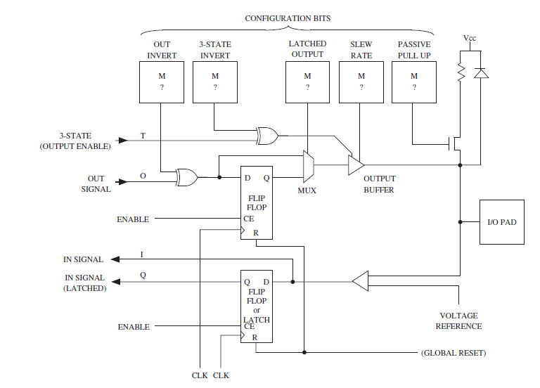
Consider the following programmable I/O block:Highlight the connections to configure this I/O block as an INPUT pin. Specify the five configuration bits. CONFIGURATION BITS Vcc OUT 3-STATE LATCHED SLEW PASSIVE OUTPUT INVERT INVERT RATE PULL UP M M ? 3-STATE т (OUTPUT ENABLE) OUT OUTPUT SIGNAL
Design the correction circuit for a BCD adder that computes Zdigit 0 and C for S0. This correction circuit adds 0110 to S0 if S0 > 9. This is the same as adding 0AA0 to S0, where A = 1 if S0 > 9. Draw a block diagram for the correction circuit using one full adder, three half adders, and a
(a) If gate delays are 5ns, what is the delay of the fastest 4-bit ripple carry adder? (b) If gate delays are 5ns, what is the delay of the fastest 4-bit adder? What kind of adder will it be?
Develop a Verilog model for a 16-bit carry look-ahead adder utilizing the 4-bit adder from Figure 4-10 as a module.
Showing 100 - 200
of 323
1
2
3
4
Step by Step Answers
![| X] XX Function | X,]X Function X, generator OX FF X generator FF O CE QX CE So LUT4 M1 х, LUT4 X4 Y1 YlY Function Y g](https://dsd5zvtm8ll6.cloudfront.net/si.question.images/images/question_images/1547/1/1/7/3545c37232a38d6e1547099978277.jpg)
![always @ (posedge CLK) begin if (CLR) else if (Ld) else if (LS) end Ld Q <= 4'b0000; Q <= D; Q <= {Q[2:0], Rin}; LS Left](https://dsd5zvtm8ll6.cloudfront.net/si.question.images/images/question_images/1546/8/6/4/2725c3346904862f1546846892418.jpg)