New Semester
Started
Get
50% OFF
Study Help!
--h --m --s
Claim Now
Question Answers
Textbooks
Find textbooks, questions and answers
Oops, something went wrong!
Change your search query and then try again
S
Books
FREE
Study Help
Expert Questions
Accounting
General Management
Mathematics
Finance
Organizational Behaviour
Law
Physics
Operating System
Management Leadership
Sociology
Programming
Marketing
Database
Computer Network
Economics
Textbooks Solutions
Accounting
Managerial Accounting
Management Leadership
Cost Accounting
Statistics
Business Law
Corporate Finance
Finance
Economics
Auditing
Tutors
Online Tutors
Find a Tutor
Hire a Tutor
Become a Tutor
AI Tutor
AI Study Planner
NEW
Sell Books
Search
Search
Sign In
Register
study help
sciences
digital systems design
Digital Systems Design Using Verilog 1st edition Charles Roth, Lizy K. John, Byeong Kil Lee - Solutions
Derive generates, propagates, group generates, group-propagates, and the final sum and carry out for the 16-bit carry look-ahead adder of Figure 4-9, while adding 0101 1010 1111 1000 and 0011 1100 1100 0011.
(a) Write a Verilog module that describes one bit of a full adder with accumulator. The module should have two control inputs, Ad and L. If Ad = 1, the Y input (and carry input) are added to the accumulator. If L = 1, the Y input is loaded into the accumulator.(b) Using the module defined in (a),
(a) Implement the traffic-light controller of Figure 4-14 using a module 13 counter with added logic. The counter should increment every clock, with two exceptions. Use a ROM to generate the outputs.(b) Write a Verilog description of your answer to (a). (c) Write a test bench for part (b) and
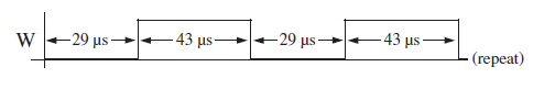
Write synthesizable Verilog code that will generate the given waveform (W). Use a single always block. Assume that a clock with a 1 μs period is available as an input. -43 μs -29 μs+ -43 μs 29 μs. - (гереat)
A BCD adder adds two BCD numbers (each of range 0 to 9) and produces the sum in BCD form. For example, if it adds 9 (1001) and 8 (1000) the result would be 17 (1 0111). Implement such a BCD adder using a 4-bit binary adder and appropriate control circuitry. Assume that the two BCD numbers are
Write Verilog code for a shift register module that includes a 16-bit shift register, a controller, and a 4-bit down counter. The shifter can shift a variable number of bits depending on a count provided to the shifter module. Inputs to the module are a number N (indicating shift count) in the
(a) Figure 4-12 shows the block diagram for a 32-bit serial adder with accumulator. The control circuit uses a 5-bit counter, which outputs a signal K = 1 when it is in state 11111. When a start signal (St) is received, the registers should be loaded. Assume that St will remain 1 until the addition
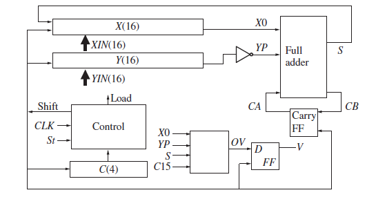
A block diagram for a 16-bit 2€™s complement serial subtracter is given here. When St = 1, the registers are loaded and then subtraction occurs. The shift counter, C, produces a signal C15 = 1 after 15 shifts. V should be set to 1 if an overflow occurs. Set the carry flip-flop to 1 during
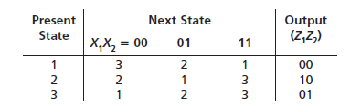
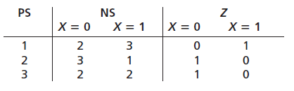
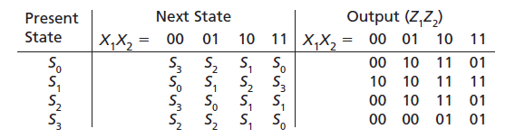
(a) Construct an SM chart equivalent to the following state table. Test only one variable in each decision box. Try to minimize the number of decision boxes.(b) Write a Verilog description of the state machine based on the SM chart. Next State Output (Z,Z,) 00 01 10 Present State х,X - 11 10
This problem involves the design of a BCD-to-binary converter. Initially a 3-digit BCD number is placed in the A register. When an St signal is received, conversion to binary takes place and the resulting binary number is stored in the B register. At each step of the conversion, the entire BCD
This problem involves the design of a circuit that finds the square root of an 8-bit unsigned binary number N using the method of subtracting out odd integers. To find the square root of N, we subtract 1, then 3, then 5, and so on, until we can no longer subtract without the result going negative.
This problem concerns the design of a multiplier for unsigned binary numbers that multiplies a 4-bit number by a 16-bit number to give a 20-bit product. To speed up the multiplication, a 4-by-4 array multiplier is used so that we can multiply by 4 bits in one clock time instead of by only 1 bit at
(a) Estimate how many AND gates and adders will be required for a 16-bit × 16-bit array multiplier.(b) What is the longest delay in a 16 × 16 array multiplier, assuming an AND gate delay is tg, and an adder delay (full adder and half adder) is tad?
(a) Draw the organization of an 8 × 8 array multiplier and calculate how many full adders, half adders, and AND gates are required.(b) Highlight the critical path in your answer to (a). (If there are many equivalent ones, highlight any one of them).(c) What is the longest delay in an 8 × 8 array
An n × n array multiplier, as in Figure 4-29, takes 3n - 4 adder delays + 1 gate delay to calculate a product. Design an array multiplier that is faster than this for n > 4. (Instead of passing carry output to the left adder, pass it to the diagonally lower one, speeding up the critical path.
The block diagram for a multiplier for signed (2’s complement) binary numbers is shown in Figure 4-33. Give the contents of the A and B registers after each clock pulse when multiplicand = -1/8 and multiplier = -3/8.
In Section 4.10 we developed an algorithm for multiplying signed binary fractions, with negative fractions represented in 2’s complement.(a) Illustrate this algorithm by multiplying 1.0111 by 1.101.(b) Draw a block diagram of the hardware necessary to implement this algorithm for the case where
The objective of this problem is to use Verilog to describe and simulate a multiplier for signed binary numbers using Booth€™s algorithm. Negative numbers should be represented by their 2€™s complement. Booth€™s algorithm works as follows, assuming each number is n
Design a multiplier that will multiply two 16-bit signed binary integers to give a 32-bit product. Negative numbers should be represented in 2’s complement form. Use the following method: First complement the multiplier and multiplicand if they are negative, multiply the positive numbers, and
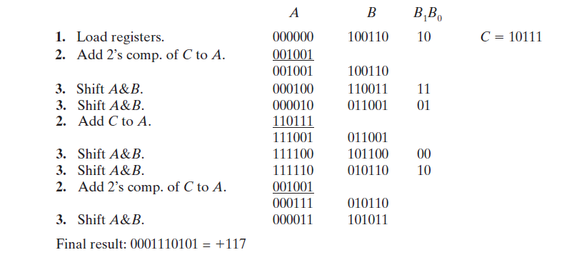
This problem involves the design of a parallel adder-subtracter for 8-bit numbers expressed in sign and magnitude notation. The inputs X and Y are in sign and magnitude, and the output Z must be in sign and magnitude. Internal computation may be done in either 2’s complement or 1’s complement
Four pushbuttons (B0, B1, B2, and B3) are used as inputs to a logic circuit. Whenever a button is pushed, it is debounced, after which the circuit loads the button number in binary into a 2-bit register (N). For example, if B2 is pushed, the register output becomes N = 102. The register holds this
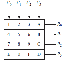
Design a 4 × 4 keypad scanner for the following keypad layout.(a) Assuming only one key can be pressed at a time, find the equations for a number decoder given R3-0 and C3-0, whose output corresponds to the binary value of the key. For example, the F key will return N3-0 = 1111 in
This problem concerns the design of a divider for unsigned binary numbers that will divide a 16-bit dividend by an 8-bit divisor to give an 8-bit quotient. Assume that the start signal (ST = 1) is 1 for exactly one clock time. If the quotient would require more than 8 bits, the divider should stop
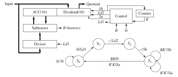
A block diagram and state graph for a divider for unsigned binary numbers is shown subsequently. This divider divides a 16-bit dividend by a 16-bit divisor to give a 16-bit quotient. The divisor can be any number in the range 1 to 216- 1. The only case where an overflow can occur is when the
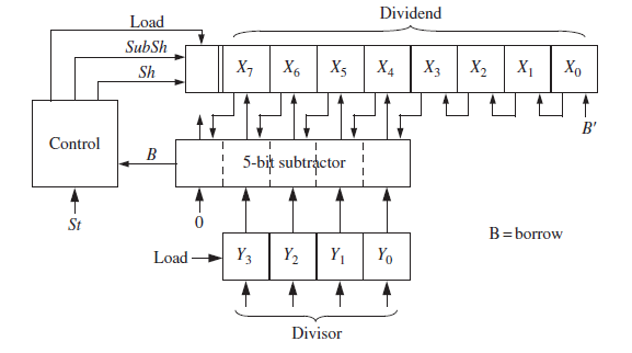
A block diagram for a divider that divides an 8-bit unsigned number by a 4-bit unsigned number to give a 4-bit quotient is shown subsequently. The Xi inputs to the subtractors are shifted over one position to the left. This means that the shift-and-subtract operation can be completed in one clock
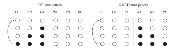
An older model Thunderbird car has three left (LA, LB, LC) and three right (RA, RB, RC) tail lights, which flash in unique patterns to indicate left and right turns.Design a Moore sequential circuit to control these lights. The circuit has three inputs: LEFT, RIGHT, and HAZ. LEFT and RIGHT come
Design a sequential circuit to control the motor of a tape player. The logic circuit will have five inputs and three outputs. Four of the inputs are the control buttons on the tape player. The input PL is 1 if the play button is pressed, the input RE is 1 if the rewind button is pressed, the input
Complete the following Verilog code to implement a test bench for the sequential circuit SMQ1. Assume that the Verilog code for the SMQ1 sequential circuit module is already available. Use a clock with a 50-ns half period. Your test bench should test the circuit for the input sequence X = 1, 0, 0,
Write a test bench to test the counter of Problem 2.48. The test bench should generate a clock with a 100-ns period. The counter should be loaded on the first clock, then it should count for 5 clocks, then it should do nothing for 2 clocks, then it should continue counting for 10 clocks. The test
Write a Verilog test bench that will test the Verilog code for the sequential circuit of Figure 2-58. Your test bench should generate all 10 possible input sequences (0000, 0001, 0010, . . .,1001) and should verify that the output sequences are correct. Remember that the components have a 10-ns
Write Verilog code to test a Mealy sequential circuit with one input (X) and one output (Z). The code should include the Mealy circuit as a component. Assume the Mealy circuit changes state on the rising edge of CLK. Your test code should generate a clock with a 100-ns period. The code should apply
A is an array of 20 4-bit registers. Write Verilog code that finds the largest register in the array,(a) Using a for loop.(b) Using a while loop.
Implement a 3-to-8 decoder using a LUT. Give the LUT truth table and write the Verilog code. The inputs should be A, B, and C, and the output should be an 8-bit unsigned vector.
(a) Write a Verilog module for a LUT with four inputs and three outputs. The 3-bit output should be a binary number equal to the number of 1s in the LUT input.(b) Write a Verilog module for a circuit that counts the number of 1s in a 12-bit number. Use three of the modules from (a) along with
What device does the following Verilog code represent?reg Qtmp;always @(CLK,RST)beginif(RST == 1'b1)Qtmp = 1'b0;else if(CLK == 1'b1 && T == 1'b1)Qtmp = ~Qtmp;else beginendQ <= Qtmp;end
When the following Verilog code is simulated, A is changed to 1 at time 5ns. Make a table that shows all changes in A, B, and D and the times at which they occur through time = 40 ns. module Q1F00(A)inout A;reg B,C;wire D;assign #10 D = A ^ B;always @(D)beginC = ~D;if(C == 1'b1)A <= #15
What is wrong with the following model of a 4-to-1 MUX? (It is not a syntax error.)reg [1:0]sel;always @(A,B,I0,I1,I2,I3)beginsel = 0;if(A == 1'b1)sel = sel + 1;elsebeginendif(B == 1'b1)sel = sel + 2;elsebeginendcase(sel)0:beginF = I0;end1:beginF = I1;end2:beginF = I2;end3:beginF = I3;endendcaseend
In the following code, state and nextstate are integers with a range of 0 to 2.always @(state,X)begincase(state)0:beginif(X == 1'b1)nextstate = 2'b01;end1:beginif(X == 1'b0)nextstate = 2'b10;end2:beginif(X == 1'b1)nextstate = 2'b00;endendcaseend(a) Explain why a latch would be created when the code
Write Verilog code to implement the following state table. Use two always blocks. State changes should occur on the falling edge of the clock. Implement the Z1and Z2outputs using concurrent conditional statements. Assume that the combinational part of the sequential circuit has a propagation delay
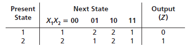
A Moore sequential machine with two inputs (X1and X2) and one output (Z) has the following state table:Write Verilog code that describes the machine at the behavioral level. Assume that state changes occur 10ns after the falling edge of the clock and output changes occur 10 ns after the state
(a) Write a behavioral Verilog description of the state machine that you designed in Problem 1.14. Assume that state changes occur on the falling edge of the clock pulse. Use a case statement together with if-then-else statements to represent the state table. Compile and simulate your code using
(a) Write a behavioral Verilog description of the state machine you designed in Problem 1.13. Assume that state changes occur on the falling edge of the clock pulse. Instead of using if-then-else statements, represent the state table and output table by arrays. Compile and simulate your code using
Examine the following Verilog code and answer the following questionsmodule Problem(X,CLK,Z1,Z2);input X,CLK;output Z1,Z2;reg [1:0]State,Nextstate;initialbeginState = 2'b00;Nextstate = 2'b00;endalways @(State,X)begincase(State)0:beginif(X == 1'b0)beginZ1 = 1'b1;Z2 = 1'b0;Nextstate = 2'b00;endelse
A synchronous 4-bit UP/DOWN binary counter has a synchronous clear signal CLR and a synchronous load signal LD. CLR has higher priority than LD. Both CLR and LD are active high. D is a 4-bit input to the counter, and Q is the 4-bit output from the counter. UP is a signal that controls the
Complete the following Verilog code to implement a counter that counts in the following sequence: Q = 1000, 0111, 0110, 0101, 0100, 0011, 1000, 0111, 0110, 0101, 0100, 0011, … (repeats). The counter is synchronously loaded with 1000 when Ld8 = 1. It goes through the prescribed sequence when
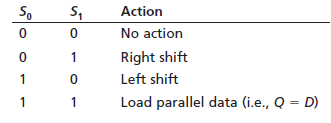
Consider the following 8-bit bidirectional synchronous shift register with parallel load capability. The notation used to represent the input/output pins is explained as follows:CLR Asynchronous Clear, which overrides all other inputsQ(7:0) 8-bit outputD(7:0) 8-bit inputS0, S1mode control inputsLSI
Write a Verilog model for a 74HC192 synchronous 4-bit up/down counter. Ignore all timing data. Your code should contain a statement of the form always @(DOWN,UP, CLR, LOADB).
A synchronous (4-bit) up/down decade counter with output Q works as follows: All state changes occur on the rising edge of the CLK input, except the synchronous clear (CLR). When CLR = 0, the counter is reset regardless of the values of the other inputs. If the LOAD input is 0, the data input
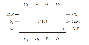
A description of a 74194 4-bit bidirectional shift register follows. The CLRb input is asynchronous and active low and overrides all the other control inputs. All other state changes occur following the rising edge of the clock. If the control inputs S1 = S0 = 1, the register is loaded in
Write a Verilog module that describes a 16-bit serial-in, serial-out shift register with inputs SI (serial input), EN (enable), CK (clock, shifts on rising edge), and a serial output (SO).
A 4-bit magnitude comparator chip (e.g., 74LS85) compares two 4-bit numbers A and B and produces outputs to indicate whether A < B, A = B, or A > B. There are three output signals to indicate each of the foregoing conditions. Note that exactly one of the output lines will be high and the
Giveninteger A = 8'shA5;integer B = 8'shB6;integer C = 8'hA5;integer D = 8'hB6;reg signed [31:0] S;Evaluatei. S = A + B;ii. S = A + B + 0;iii. S = C + D;iv. S = C + D + 0;v. S = A + D;vi. S = A + D + 0;
Givenreg [3:0] A = 4'b1101;reg [2:0] B = 3'b111;reg signed [3:0] C = 4'b1101;reg signed [2:0] D = 3'b111;reg signed [7:0] S;Evaluatei. S = A + B;ii. S = A + B + 0;iii. S = C + D;iv. S = C + D + 0;v. S = A + D;vi. S = A + D + 0;
Write a Verilog description of an SR latch.(a) Use a conditional assignment statement (i.e., a behavioral description).(b) Use the characteristic equation in the Verilog description.(c) Use the logic gate level structure of an SR latch in the model.
(a) Write at least two different Verilog modules that are equivalent to the following pseudo code:A = B1 when C = 1 else B2 when C = 2 else B3 when C = 3 else 0;(b) Draw a circuit to implement the following statement,A = B1 when C1 = 1 else B2 when C2 = 1 else B3 when C3 = 1else 0;
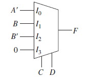
(a) Write a conditional signal assignment statement to represent the 4-to-1 MUX shown subsequently. Assume that there is an inherent delay in the MUX that causes the change in output to occur 10 ns after a change in input.(b) Repeat (a) using an if-else statement.(c) Repeat (a) using a case
Draw the circuit represented by the following Verilog process:always @(clk,clr)beginif(clr == 1'b1)Q <= 1'b0;else if(clk == 1'b0 && CE == 1'b1)beginif(C == 1'b0)Q <= A & B;elseQ <= A | B;endendWhy is clr on the sensitivity list whereas C is not?
Implement the following Verilog code using these components: D flip-flops with clock enable, a multiplexer, an adder, and any necessary gates. Assume that Ad and Ora will never be 1 at the same time and enable the flip-flops only when Ad or Ora is 1.module module1(A,B,Ad,Ora,clk,C);input
Consider the following Verilog code:module Q3(A,B,C,F,Clk,E);input A,B,C,F,Clk;output reg E;reg D,G;initialbeginE = 1'b0;D = 1'b0;G = 1'b0;endalways @(posedge Clk)beginD <= A & B & C;G <= ~A & ~B;E <= D | G | F;endendmodule(a) Draw a block diagram for the circuit (no gates and
If A = 101, B = 011, and C = 010, what are the values of the following statements? Assume A, B, and C are of reg type. Assume as many bits as necessary for the result.(a) {A,B} | {B,C}(b) A >> 2(c) A >>> 2(d) {A,(~B)} == 111110(e) A | B & C
In the following Verilog Code, A, B, C, and D are registers that are 0 at time = 4 ns. If A changes to 1 at time 5 ns, make a table showing the values of A, B, C, and D as a function of time until time = 18 ns. Include deltas. Indicate the times at which each process begins executing.always
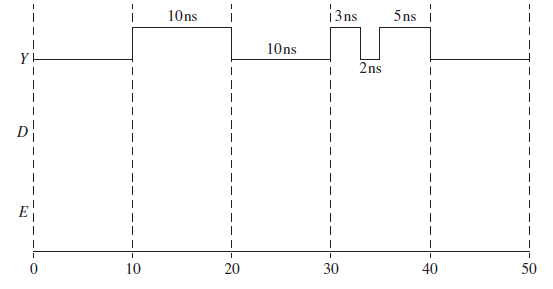
Given the following timing waveform for Y, draw D and E.wire #3 D; // net delay on wire Dassign #5 D = Y; // statement 1 - inertial delaywire #5 E; // net delay on wire Eassign #3 E = Y; // statement 1 - inertial delay i3ns 10ns 5ns 10ns 2ns 10 30 40 50 20
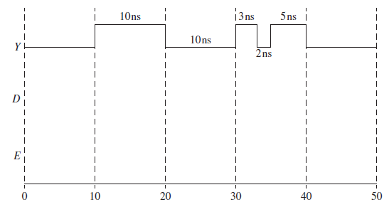
Given the following timing waveform for Y, draw D and E.wire #4 D; // net delay on wire Dassign #6 D = Y; // statement 1 2 inertial delaywire #6 E; // net delay on wire Eassign #4 E = Y; // statement 1 - inertial delay 13ns 5ns i 10ns | 10ns 2 ns 10 30 40 50 20
Assuming B is driven by the simulator command:force B 0 0, 1 4, 0 10, 1 15, 0 20, 1 30, 0 40Draw a timing diagram illustrating A, B, and C if the following statement is executed:(a) always @(A,B)begin#5 C <= A && B;end(b) always @(A,B)begin#5 C = A && B;end(c) always
Assuming B is driven by the simulator command:force B 0 0, 1 4, 0 10, 1 15, 0 20, 1 30, 0 40Draw a timing diagram illustrating A, B, and C if the following concurrent statements are executed:always @(B)beginA <= #5 B;endassign #5 C <= B;
Assuming B is driven by the simulator command:force B 0 0, 1 10, 0 15, 1 20, 0 30, 1 35Draw a timing diagram illustrating A, B, and C if the following concurrent statements are executed:always @(B)beginA = #5 B;endassign #8 C = B;
For the following Verilog code, assume that D changes to 1 at time 5 ns. Give the values of A, B, C, D, E, and F each time a change occurs. That is, give the values at time 5 ns, 5 + D, 5 + 2D, and so forth. Carry this out until 20 steps have occurred, until no further change occurs, or until a
What is wrong with the following code for a half adder that must add if add signal equals 1?always @(x)beginif (add == 1)beginsum = x ^ y;carry = x & y;endelsebeginsum = 0;carry = 0;endend
(a) Assume D1 = 0, D2 = 5, and D1 changes to 1 at time = 10ns. What are the values of D1 and D2 after the following code has been executed once? Do the values of D1 and D2 swap?always @ (D1)beginD2 <= D1;D1 <= D2;End(b) Assume D1 = 0, D2 = 5, and D1 changes to 1 at time = 10 ns.
Draw the hardware obtained if the following two modules are synthesized and describe the differences.module reg3 (Q1,Q2,Q3,Q4,A,CLK);input A;input CLK;output Q1,Q2,Q3,Q4;reg Q1,Q2,Q3,Q4;// firstalways @(posedge CLK)beginQ1 <= A;Q2 <= Q1;Q3 <= Q2;Q4 <= Q3;endendmodulemodule reg3
Draw the hardware obtained if the following code is synthesized:module reg3 (Q1,Q2,Q3,Q4, A,CLK);input A;input CLK;output Q1,Q2,Q3,Q4;reg Q1,Q2,Q3,Q4;always @(posedge CLK)beginQ1 = A;Q2 = Q1;Q3 = Q2;Q4 = Q3;endendmodule
Givenreg [7:0] C;reg signed [7:0] D;reg [7:0] A = 8'shD5;Evaluatei. C = A >> 4ii. C = A >>> 4iii. C = A << 4iv. C = A <<< 4v. D = A >> 4vi. D = A >>> 4vii. D = A << 4viii. D = A <<< 4
Givenreg [7:0] C;reg signed [7:0] D;reg [7:0] A = 8'hD5;Evaluatei. C = A >> 4ii. C = A >>> 4iii. C = A << 4iv. C = A <<< 4v. D = A >> 4vi. D = A >>> 4vii. D = A << 4viii. D = A <<< 4
EvaluateA >> 4A >>> 4A << 4A <<< 4given(a) reg signed [7:0] A = 8'hC7;(b) reg [7:0] A = 8'hA5;(c) reg signed [7:0] A = 8'hC7;(d) integer signed A = 8'hC7;(e) integer A = 8'hC7;(f) integer A = 8'shC7;(g) integer signed A = 8'shC7;(h) integer signed A = 32'hFFFFFFC7;
Givenreg [7:0] C;reg signed [7:0] D;reg signed [7:0] A = 8'hD5;evaluatei. C = A >> 4ii. C = A >>> 4iii. C = A << 4iv. C = A <<< 4v. D = A >> 4vi. D = A >>> 4vii. D = A << 4viii. D = A <<< 4
Givenwire a = 1'b0;wire [1:0] b = 2'b10;wire [2:0] c = 3'b101;Evaluatei. { 4{a} }ii. { 4{a}, 2{b} }iii. { 4{a}, c}
Givenwire a = 1'b1;wire [1:0] b = 2'b10;wire [2:0] c = 3'b101;Evaluatei. {b, c}ii. {a, b, c, 2'b01}iii. {a, b[0], c[1]}
Draw the hardware obtained if the following code is synthesized:module reg3 (Q1,Q2,Q3,Q4, A,CLK);input A;input CLK;output Q1,Q2,Q3,Q4;reg Q1,Q2,Q3,Q4;always @(posedge CLK)beginQ4 = Q3;Q3 = Q2;Q2 = Q1;Q1 = A;endendmodule
In the following Verilog process A, B, C, and D are all registers that have a value of 0 at time = 10 ns. If E changes from 0 to 1 at time = 20 ns, specify the time(s) at which each signal will change and the value to which it will change. List these changes in chronological order.always @(E)beginA
In the following Verilog process A, B, C, and D are all registers that have a value of 0 at time = 10ns. If E changes from 0 to 1 at time = 20ns, specify the time(s) at which each signal will change and the value to which it will change. List these changes in chronological
An inhibited toggle flip-flop has inputs I0, I1, T, and Reset and outputs Q and QN. Reset is active high and overrides the action of the other inputs. The flip-flop works as follows: If I0 = 1, the flip-flop changes state on the rising edge of T; if I1 = 1, the flip-flop changes state on the
A DD flip-flop is similar to a D flip-flop, except that the flip-flop can change state (Q+ = D) on both the rising edge and the falling edge of the clock input. The flip-flop has a direct reset input, R, and R = 0 resets the flip-flop to Q = 0 independent of the clock. Similarly, it has a direct
An M-N flip-flop responds to the falling clock edge as follows:If M = N = 0, the flip-flop changes state.If M = 0 and N = 1, the flip-flop output is set to 1.If M = 1 and N = 0, the flip-flop output is set to 0.If M = N = 1, no change of flip-flop state occurs.The flip-flop is cleared
Write a Verilog description of an S-R latch using an always block.
(a) What device does the following Verilog code represent?always @(CLK, Clr, Set)beginif(Clr == 1'b1)Q <= 1'b0;else if(Set == 1'b1)Q <= 1'b1;else if(CLK == 1'b0)Q <= D;else beginendend(b) What happens if Clr = Set = 1 in the device in part a?
In the following Verilog code, A, B, C, and D are 0 at time 10 ns. If D changes to 1 at 20 ns, specify the times at which A, B, and C will change and the values they will take.(a) always @(D)begin#5 A <= 1;B <= A + 1;#10 C <= B;end(b) always @(D)beginA <= #5 1;B <= A + 1;C
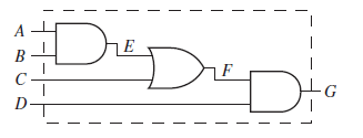
Write Verilog code for the following circuit. Assume that the gate delays arenegligible.(a) Using concurrent statements.(b) Using an always block with sequential statements. No latches should be generated. DeDeD B
(a) Write Verilog code for a full subtracter using logic equations.(b) Write Verilog code for a 4-bit subtracter using the module defined in (a) as a component.
Write a Verilog description of the following combinational circuit using concurrent statements. Each gate has a 5-ns delay, excluding the inverter, which has a 2-ns delay. C - ABCDAR
Given the concurrent Verilog statements:assign #3 B = A && C;assign #2 C = !B;(a) Draw the circuit the statements represent.(b) Draw a timing diagram if initially A = B = 0 and C = 1, and A changes to 1 at time 5ns.
(a) Which of the following are legal Verilogidentifiers? 123A, A_123, _A123, $A123_, c1__c2, and, and1(b) Which of the following Verilogidentifiers are equivalent? aBC, ABC, Abc, abc
(a) What do the acronyms HDL and FPGA stand for?(b) How does a hardware description language like Verilog differ from an ordinary programming language?(c) What are the advantages of using a hardware description language as compared with schematic capture in the design process?
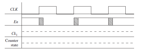
A simple binary counter has only a clock input (Ck1). The counter increments on the rising edge of Ck1. (a) Show the proper connections for a signal En and the system clock (CLK), so that when En = 1, the counter increments on the rising edge of CLK and when En = 0, the counter does not change
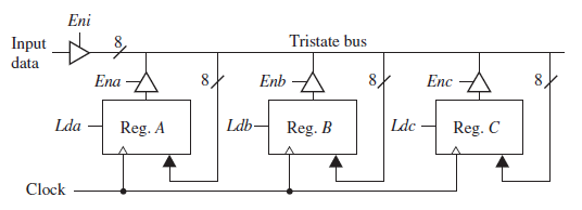
Referring to Figure 1-56, specify the values of Eni, Ena, Enb, Enc, Lda, Ldb, and Ldc so that the data stored in Reg. C will be copied into Reg. A and Reg. B when the circuit is clocked. Eni Input N 8 Tristate bus data 8 8 Enc Ena Enb Ldb- Ldc - Reg. A Reg. B Reg. C Lda Clock
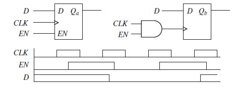
(a) Do the following two circuits have essentially the same timing?(b) Draw the timing for Qaand Qbgiven the timing diagram.(c) If your answer to (a) is no, show what change(s) should be made in the second circuit so that the two circuits have essentially the same timing (do not change the
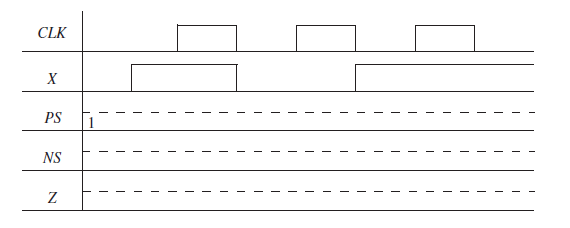
A Mealy sequential machine has the following state table:Complete the following timing diagram. Clearly mark on the diagram the times at which you should read the values of Z. All state changes occur after the rising edge of the clock. Assume the machine is initialized to state 1 NS PS X%3D
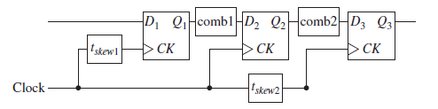
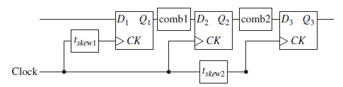
Consider the following circuit where the combinational circuit is represented by COMB and clock skew is represented by tskew. Given the following parameters: FF setup time = 10 nsFF hold time = 2 nsFF propagation delay = 12 to 20 nsTcomb1 = 5 ns to 7 nsTcomb2 = 6 ns to 11 ns(a) What
Consider the following circuit where the combinational circuit is represented by COMB and clock skew is represented by tskew.Given the following parameters:FF setup time = 20 ns FF hold time = 10 nsFF propagation delay = 5 to 10 nsTcomb 1 = 5 ns to 7 nsTcomb 2 = 6 ns to 11 ns(a) What is the
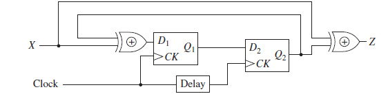
In the following circuit, the XOR gate has a delay in the range of 2 to 16 ns. The D flip-flop has a propagation delay from clock to Q in the range 12 to 24 ns. The setuptime is 8 ns, and the hold time is 4 ns.(a) Assume delay = 0 ns and compute the maximum frequency at which this circuit can be
In the following circuit, the XOR gate has a delay in the range of 2 to 16 ns. The D flip-flop has a propagation delay from clock to Q in the range 12 to 24 ns. The setup time is 8 ns, and the hold time is 4 ns. (a) What is the minimum clock period for proper operation of the circuit?(b) What
Showing 200 - 300
of 323
1
2
3
4
Step by Step Answers
![Ld Ad Sh4 A (24 bits) St 16 8- 8- Control Mult. 8-bit adder Done 4x4 array multiplier Mcand A[3:0]](https://dsd5zvtm8ll6.cloudfront.net/si.question.images/images/question_images/1546/8/7/5/0145c3370867380d1546857635623.jpg)